Semiconductor relay

a relay and semiconductor technology, applied in pulse generators, pulse techniques, instruments, etc., can solve the problems of inability to switch at high speed, large current cannot be supplied from the controller,

Active Publication Date: 2009-08-18
ADVANTEST CORP
View PDF4 Cites 1 Cited by
  • Summary
  • Abstract
  • Description
  • Claims
  • Application Information

AI Technical Summary

Problems solved by technology

Consequently, the proposed semiconductor relay has a problem that large current cannot be supplied from the controller 120, and the MOSFETs 131, 132 cannot be switched at high speed.

Method used


Image

  • Semiconductor relay
  • Semiconductor relay
  • Semiconductor relay

Examples


first embodiment

A First Embodiment

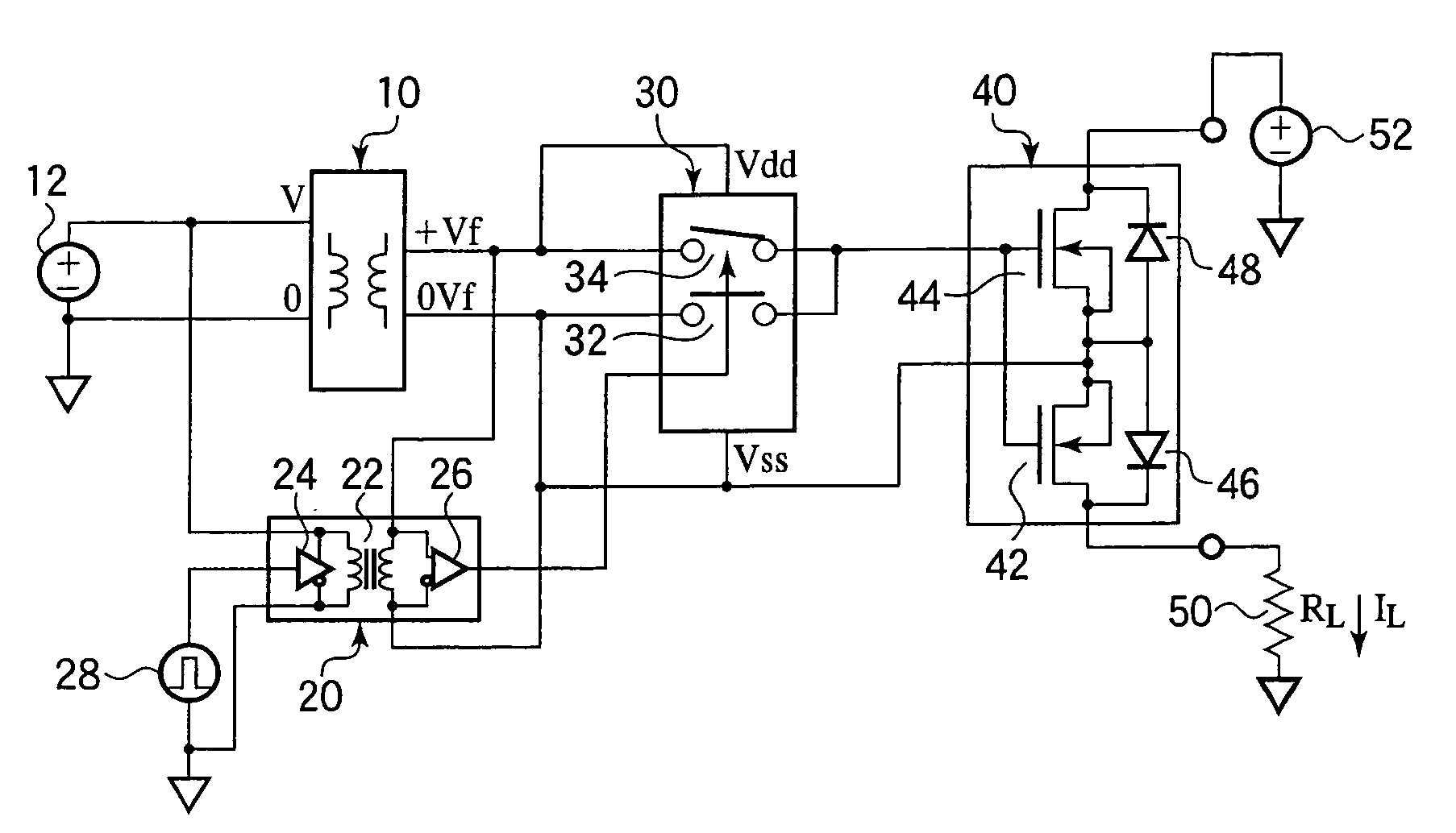
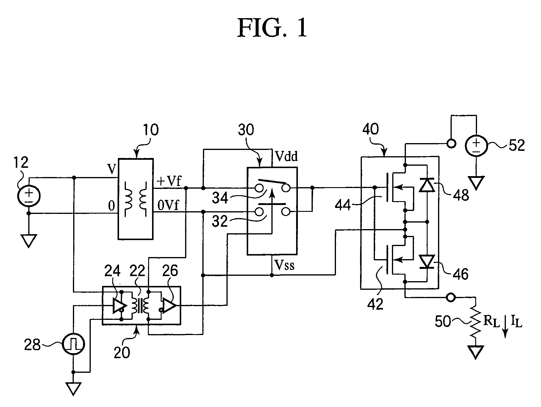
[0026]The semiconductor relay according to a first embodiment of the present invention will be explained with reference to FIG. 1. FIG. 1 is a circuit diagram of the semiconductor relay according to the present embodiment.

[0027]First, the constitution of the semiconductor relay according to the present embodiment will be explained.

[0028]The semiconductor relay according to the present embodiment comprises an insulated type DC / DC power supply 10 having the input and the output insulated from each other, a pulse transformer 20 having the input and the output insulated from each other, an analog switch 30 which turns on and off the circuit in accordance with the sate of an input signal, and a MOSFET circuit 40 which turns on and off a high voltage to a load.

[0029]A DC power supply 12 of V volt (e.g., 12 V) is connected to the input side of the insulated type DC / DC power supply 10. From the output side of the insulated type DC / DC power supply 10, a DC voltage of Vf vol...

second embodiment

A Second Embodiment

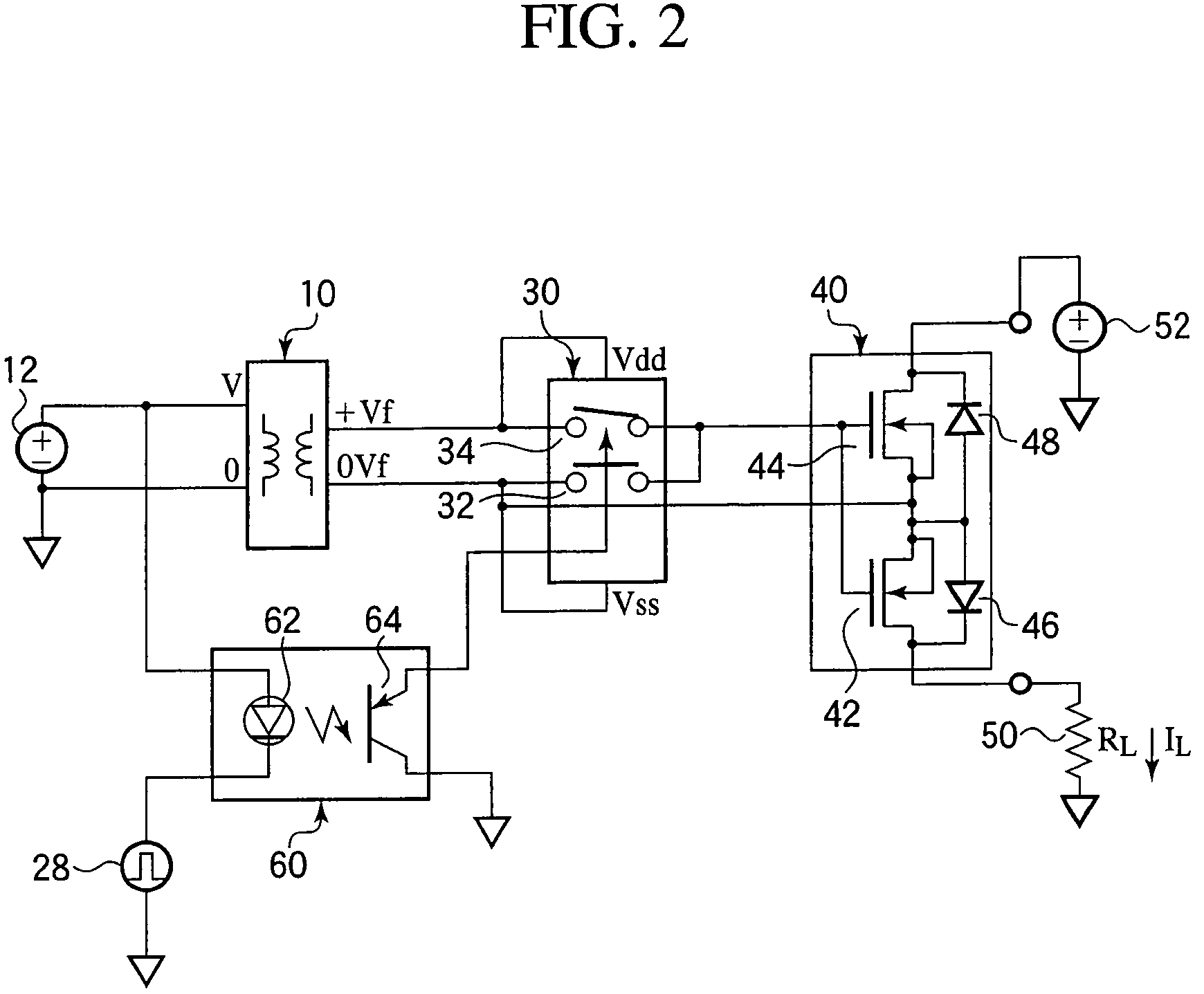
[0048]The semiconductor relay according to a second embodiment of the present invention will be explained with reference to FIG. 2. FIG. 2 is a circuit diagram of the semiconductor relay according to the present embodiment. The same members or the members of the same kinds of the present embodiment as those of the semiconductor relay according to the first embodiment are represented by the same reference numbers not to repeat or to simplify their explanation.

[0049]The constitution of the semiconductor relay according to the present embodiment will be explained.

[0050]The semiconductor relay according to the present embodiment includes a photocoupler 60 in place of the pulse transformer 20 of the semiconductor relay according to the first embodiment.

[0051]The photocoupler 60 is a coupling device combining a light emitting diode 62 and a phototransistor 64 with light as a medium and is one kind of the photoisolator.

[0052]The pulse signal source 28 is connected to the...

third embodiment

A Third Embodiment

[0064]The semiconductor relay according to a third embodiment of the present invention will be explained with reference to FIG. 3. FIG. 3 is a circuit diagram of the semiconductor relay according to the present embodiment. The same members or the members of the same kinds of the present embodiment as those of the first embodiment are represented by the same reference numbers not to repeat or to simplify their explanation.

[0065]First, the constitution of the semiconductor relay according to the present embodiment will be explained.

[0066]The semiconductor relay according to the present embodiment includes an optical coupling DC power supply 70 in place of the insulated type DC / DC power supply 10 of the semiconductor relay according to the first embodiment.

[0067]The optical coupling DC power supply 70 includes a light emitting diode 72 which emits light, a light receiving circuit 74 having a plurality of photodiodes or solar cells serially connected, and a condenser 7...


PUM


Abstract

The semiconductor relay comprises: an insulated type DC / DC power supply 10 having the input terminal and the output terminal insulated from each other; a pulse transformer 20 having the input terminal and the output terminal insulated from each other; an analog switch 30 which turns on and off the circuit in accordance with a state of an input signal; and a MOSFET circuit 40 which turns on and off a high voltage to a load 50. When a pulse signal is outputted from a pulse signal source 28, the pulse signal is outputted from the pulse transformer 20, and a state of the analog switch 30 is switched, a supply voltage is outputted from the output terminal of the analog switch 30, both the MOSFETs 42, 44 of the MOSFET circuit conduct, and a high AC voltage is applied to a load 50 from an AC power supply 52. Then, when a pulse signal is outputted from the pulse signal source 28, the pulse signal is outputted from the pulse transformer 20, the state of the analog switch 30 is switched, a ground voltage is outputted from the output terminal of the analog switch 30, both the MOSFETs 42, 44 of the MOSFET circuit are turned off, and the high AC voltage from the AC power supply 52 is not applied to the load 50.

Description

BACKGROUND OF THE INVENTION[0001]The present invention relates to a semiconductor relay, more specifically, a semiconductor relay which turn on and off high voltage at high speed.[0002]A semiconductor relay which insulates the input and the output from each other by the optical coupling mode is known as a semiconductor relay which turns on and off high voltages by small input signals.[0003]FIG. 5 illustrates a proposed semiconductor relay. This semiconductor relay includes a optical pulse generating circuit 100 which generates an optical pulse signal as a input signal, a light receiving circuit 110 which receives the optical pulse signal from the optical pulse generating circuit 100, a controller 120 which drives a MOSFET circuit 130 which will be described later in accordance with the received light signal of the light receiving circuit 110, and the MOSFET circuit 130 which is driven by the controller 120.[0004]In the optical pulse generating circuit 100, one end of a resistor 102 ...

Claims


Application Information

Patent Timeline
Patent Type & Authority Patents(United States)
IPC IPC(8): G02B27/00H01J40/14
CPCH03K17/785H03K17/6874H03K17/691H03K2217/0009H03K2217/0081H03K17/78
Inventor SATO, LEGAL REPRESENTATIVE, SHINYASATO, TADAAKISATO, NOBUHIRO
Owner ADVANTEST CORP
Why Eureka
Try Eureka