Semiconductor device and method of producing the same

a technology of semiconductors and devices, applied in the direction of semiconductor devices, bulk negative resistance effect devices, electrical appliances, etc., can solve the problems of no solution proposed, no rewriting number is guaranteed, and the volume of the phase change region is not increased

Active Publication Date: 2009-09-15
MICRON TECH INC
View PDF6 Cites 17 Cited by
  • Summary
  • Abstract
  • Description
  • Claims
  • Application Information

AI Technical Summary

Benefits of technology

[0014]It is another object of this invention to provide a method of producing a semiconductor device having a memory cell capable of carrying out stable rewriting.

Problems solved by technology

In other words, as the number of times of rewriting is increased, rewriting can not be carried out at a predetermined current level so that the number of times of rewriting may not be assured.
On the other hand, in the abovementioned patent documents, no recognition is made about such dependency upon the number of times of rewriting and, therefore, no solution is proposed.
As described above, in the above-mentioned memory element using the chalcogenide layer, there is a problem that the resistance value of the chalcogenide layer is varied as the number of times of rewriting is increased.
In other words, as the number of times of rewriting is increased, rewriting can not be carried out at a predetermined current level so that the number of times of rewriting may not be assured.
In other words, rewriting can not be carried out at a predetermined current level.
Thus, rewriting resistance or durability is not assured due to an adverse influence caused by a part of the chalcogenide layer which does not act as a phase change region in an early stage of repetition of rewriting operations.

Method used


Image

  • Semiconductor device and method of producing the same
  • Semiconductor device and method of producing the same
  • Semiconductor device and method of producing the same

Examples


first embodiment

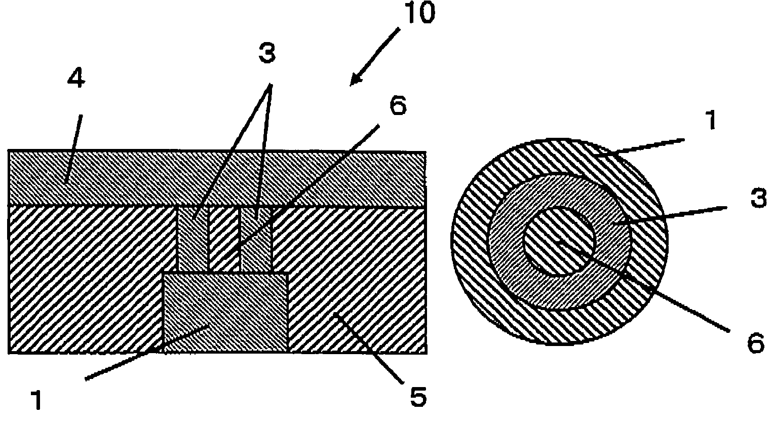
[0067]Referring to FIGS. 6 to 13, description will be made of a memory element portion of a memory cell according to a first embodiment of this invention. In the figures, those parts directly related to this invention, including a chalcogenide layer, a heater electrode, and an upper electrode, are illustrated and other parts such as transistors and wiring layers contained in a typical semiconductor device are omitted.

[0068]As illustrated in FIG. 6, a chalcogenide layer 3 according to the first embodiment is formed into a ring shape as a side wall along an inner surface of a contact hole 7 formed on a heater electrode or first electrode 1 as phase changing portion and penetrating an interlayer insulation film 5 of a thermal oxide film (SiO2). A buried insulation film 6 is filled inside the chalcogenide layer 3 of a ring shape. Surfaces of the interlayer insulation film 5, the buried insulation film 6, and the chalcogenide layer 3 are planarized or flattened by CMP (Chemical Mechanica...

second embodiment

[0078]Referring to FIG. 14, a second embodiment of this invention will be described.

[0079]As illustrated in FIG. 14, the second embodiment is different from the first embodiment in that a first insulation film 8 is formed as a side wall inside the contact hole 7 at a position between the interlayer insulation film 5 and the chalcogenide layer 3. Similar parts are designated by like reference numerals and description thereof is omitted.

[0080]A memory cell illustrated in FIG. 14 comprises the first insulation film 8 as the side wall inside the contact hole 7 formed in the interlayer insulation film 5. Inside the first insulation film 8, the chalcogenide layer 3 and the buried insulation film 6 are formed. In the structure of the second embodiment, the chalcogenide layer 3 has upper and lower surfaces contacted with the first electrode or heater electrode 1 as phase changing portion and the upper electrode 4 and a side surface contacted with the first insulation film 8 and the buried i...

third embodiment

[0083]Referring to FIG. 15, a third embodiment of this invention will be described. FIG. 15 is a sectional view of a memory element portion of a memory cell according to the third embodiment. This embodiment is different from the second embodiment in that the chalcogenide layer has a recessed structure and is further reduced in volume. As illustrated in FIG. 15, the chalcogenide layer 3 has a recessed structure lower in height than planarized surfaces of the interlayer insulation film 5, the first insulation film 8, and the buried insulation film 6. The upper electrode 4 is formed on the planarized surfaces and in a recessed portion. The chalcogenide layer 3 has side surfaces contacted with the first insulation film 8 and the buried insulation film 6 like in the second embodiment. Similar parts are designated by like reference numerals and description thereof is omitted.

[0084]Description will be made of a method of producing a semiconductor device according to the third embodiment w...


PUM


Abstract

In a semiconductor device, a phase change layer is formed as a side wall and is therefore reduced in volume. Even if the number of times of rewriting is small, the phase change layer is entirely used as a phase change region. Therefore, the phase change region is not increased in volume even if the number of times of rewriting is increased. Since the volume of the phase change region is not changed, an electric current level required for rewriting is constant. Thus, the semiconductor device having a memory cell capable of carrying out stable rewriting is obtained.

Description

[0001]This application claims priority to prior Japanese patent application JP 2005-212419, the disclosure of which is incorporated herein by reference.BACKGROUND OF THE INVENTION[0002]This invention relates to a semiconductor device and, in particular, to a semiconductor device using a phase change material as a memory element of a memory cell and a method of producing the same.[0003]A phase change memory using a phase change material is known in the art. As the phase change material, a chalcogenide material (GeSbTe) is generally used. A change in resistance value following a change in crystal structure of the chalcogenide material is used as memory information. In the phase change memory, a chalcogenide layer obtained by depositing the chalcogenide material is used as a memory element instead of a capacitance element in a typical DRAM (Dynamic Random Access Memory). The chalcogenide layer is varied in crystal structure depending upon a heating temperature and a cooling time and ex...

Claims


Application Information

Patent Timeline
Patent Type & Authority Patents(United States)
IPC IPC(8): H01L45/00H01L31/032
CPCH01L45/06H01L45/124H01L45/1691H01L45/144H01L45/126H10N70/8265H10N70/8413H10N70/231H10N70/068H10N70/8828
Inventor SATO, NATSUKI
Owner MICRON TECH INC
Why Eureka
Try Eureka