Semiconductor device and method of manufacturing the same

a technology of semiconductors and semiconductors, applied in the direction of semiconductor devices, bulk negative resistance effect devices, electrical appliances, etc., can solve the problems of difficult rewriting, achieve stable rewriting, suppress the formation of voids of ion supply sources, and change the resistance of the memory area rm

Inactive Publication Date: 2009-10-01
HITACHI LTD
View PDF9 Cites 22 Cited by
  • Summary
  • Abstract
  • Description
  • Claims
  • Application Information

AI Technical Summary

Benefits of technology

[0011]The solid electrolyte memory involves a problem that stable rewriting is difficult since the amount of the ions A in the solid electrolyte and the shape of the electrode are changed by repeating rewriting. A typical structure of a circuit device studied by us for solving the problem is to be described with reference to FIG. 3. While the supply layer for the ions A was the electrode 22 in the existent solid electrolyte memory, this is a solid electrolyte material in our memory. For example, this is Cu—Ta—S. Description is to be made to an example of Cu—Ta—S. Further, a filament forming area includes a ternary oxide. This is, for example, Cu—Ta—O. Description is to be made to an example of Cu—Ta—O. Further, the filament forming area is to be defined as an ion confinement layer. The effect obtained by the structure is to be described later. At first, by changing the ion supply source from the electrode 22 to the solid electrolyte Cu—Ta—S the total amount of ions that can be supplied is restricted, and further, a physical change such as formation of voids of the ion supply source is suppressed. Secondly, Cu and Ta of different mobilities are used as metal ions. Ta of low mobility forms a stable structure of TaS or TaO. On the other hand, Cu of high mobility changes the resistance of the memory area RM by forming and eliminating the electroconductive filament.

Problems solved by technology

The solid electrolyte memory involves a problem that stable rewriting is difficult since the amount of the ions A in the solid electrolyte and the shape of the electrode are changed by repeating rewriting.

Method used


Image

  • Semiconductor device and method of manufacturing the same
  • Semiconductor device and method of manufacturing the same
  • Semiconductor device and method of manufacturing the same

Examples


embodiment 1

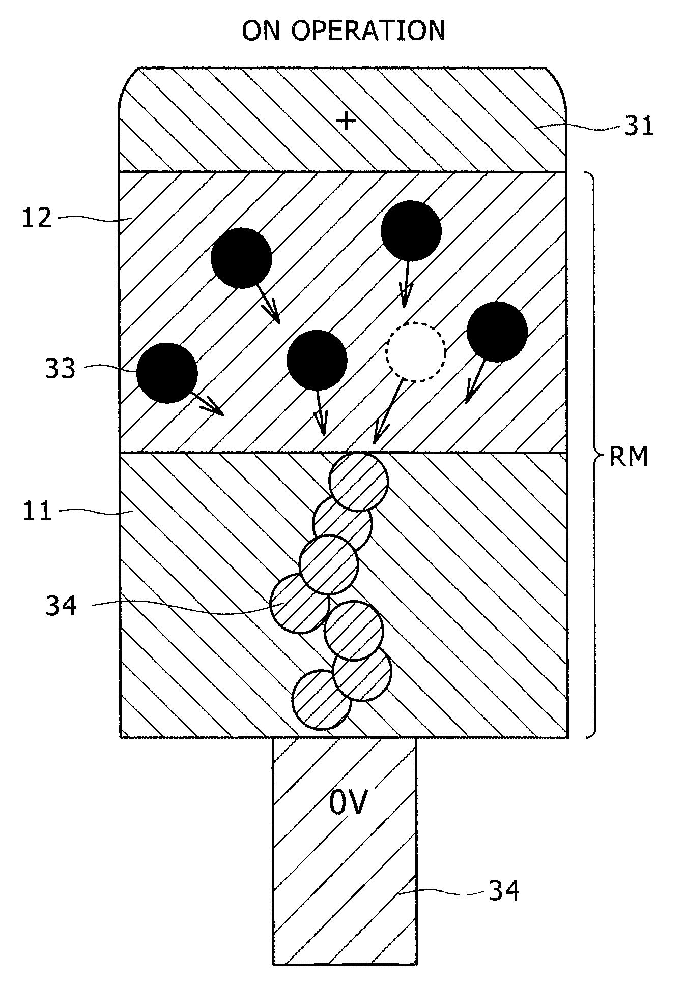
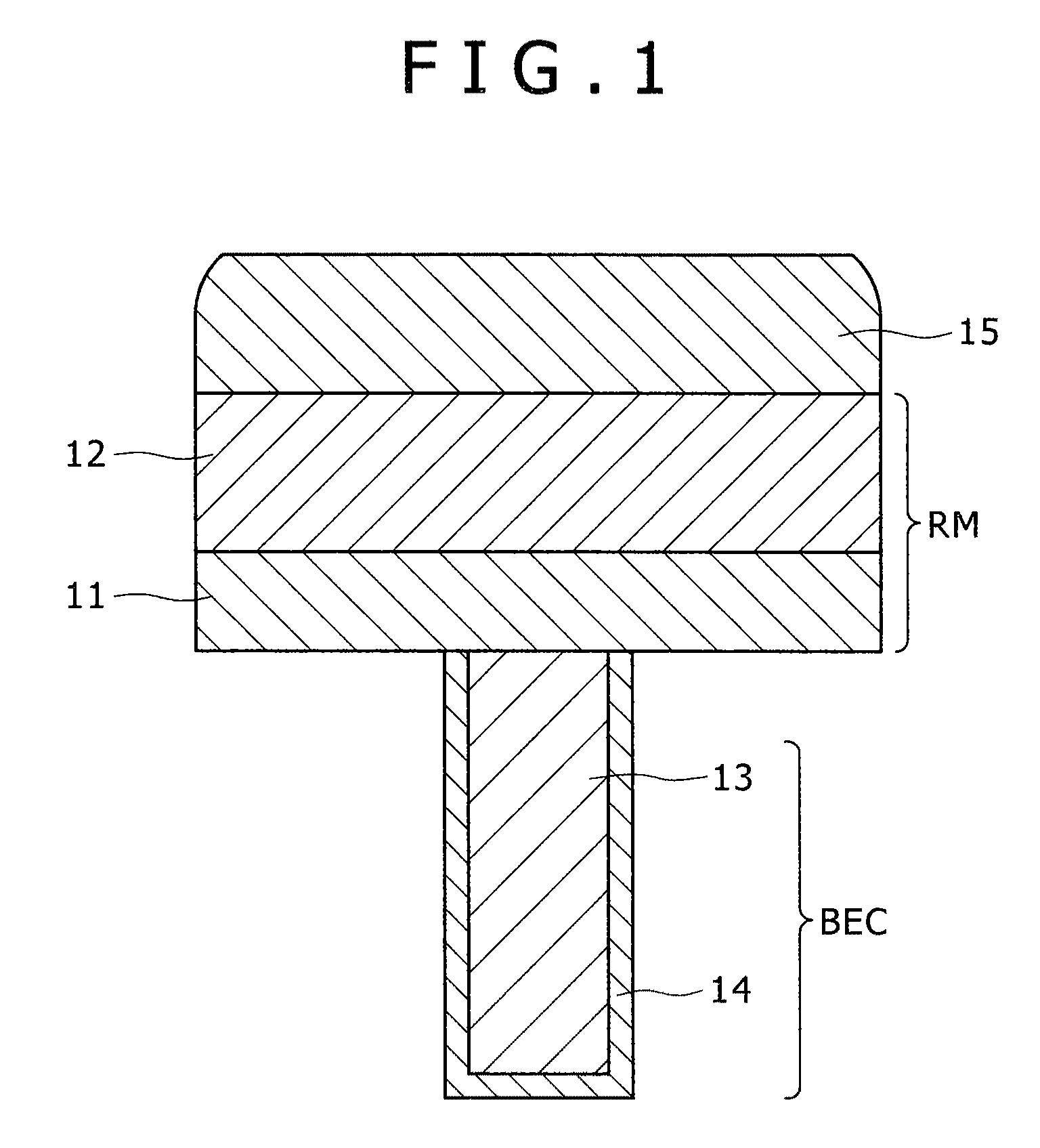
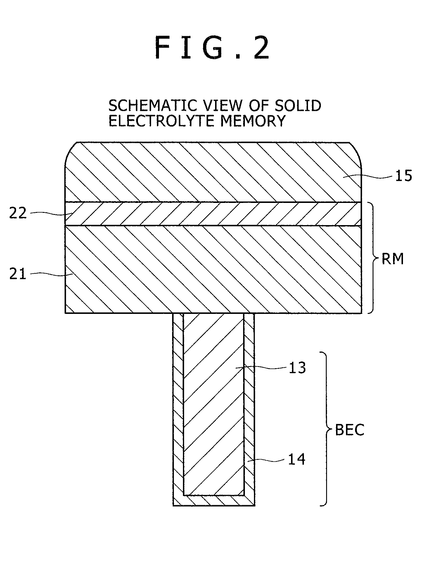
[0047]FIG. 1 is a cross sectional view showing the constitution of a memory device using a solid electrolyte material according to the first embodiment of the invention. As shown in the drawing, the memory device of the invention has a structure in which a memory area RM where an ion confinement layer 11 and an ion supply layer 12 are stacked is sandwiched between a lower electrode BEC and an upper electrode 15. The lower electrode BEC includes an adhesion layer 14 and a plug material 13. For the adhesion layer 14, TiN of excellent burying property to a hole shape of fine dimension can be used for example. As the material for the plug material 13 and the upper electrode 15, W of low electric resistance can be used. As the material for BEC, TiAlN or TiW, TiSiC, TaN, carbon cluster (carbon allotrope such as C60) as high melting materials can be used. In this case, as a method of eliminating an electroconductive filament, a method of generating Joule heat to the ion confinement layer a...

embodiment 2

[0077]This embodiment has a feature that the ion confinement layer is crystallized by laser irradiation in the Cu—Ta—O crystallization methods shown in FIG. 13.

[0078]Film formation of Cu—Ta—O is performed as described below. An amorphous Cu—Ta—O film is formed while controlling the substrate temperature upon sputtering to such a low level that Cu—Ta—O is not crystallized. Then, crystallization is performed for Cu—Ta—O by using laser irradiation.

[0079]Elevation for the temperature of the silicon wafer substrate can be mitigated by using laser irradiation not by a heat treatment using a furnace. Thus, since not only the problem that the transistor characteristics are deteriorated due to movement of a dopant in the diffusion layer can be avoided but also degradation of Low-k material can further be prevented, a Low-k material can be used for the interlayer dielectric film. By using the Low-k material, wiring delay in the semiconductor circuit can be mitigated and high speed operation c...

embodiment 3

[0083]This embodiment has a feature in crystallizing Cu—Ta—O by applying heat treatment in an electric furnace or IR furnace after forming an amorphous Cu—Ta—O film among the crystallization methods for Cu—Ta—O in FIG. 13. A fine crystal structure can be obtained by performing crystallization while taking a long time since this can suppress the crystal growing rate and, relatively, increase the probability of formation of crystal nuclei. Since this can make the number of grain boundaries on BEC uniform, effects of grain boundaries on the rewriting operation can be averaged. As a result, a semiconductor circuit device of less variation can be provided. The heat treatment time is, for example, 30 min. As described in Embodiment 1, since the crystallization temperature for Cu—Ta—O is 600° C. or higher, the heat treatment temperature is preferably 600° C. or higher.


PUM


Abstract

A solid electrolyte memory involves a problem that stable rewriting is difficult since the amount of ions in the solid electrolyte and the shape of the electrode are changed by repeating rewriting. In a semiconductor device in which information is stored or the circuit connection is changed by the change of resistance of the solid electrolyte layer, the solid electrolyte layer includes a composition, for example, of Cu—Ta—S and an ion supply layer in adjacent or close therewith as Cu—Ta—O, in which ions supplied from the ion supply layer form a conduction path in the solid electrolyte layer thereby making it possible to store information by the level of the resistance and applying the electric pulse to change the resistance, in which the ion supply layer includes crystals having, for example, a compositional ratio of: Cu—Ta—O=1:2:6 and rewriting operation can be performed stably.

Description

CLAIM OF PRIORITY[0001]The present application claims priority from Japanese patent application JP 2008-089776 filed on Mar. 31, 2008, the content of which is hereby incorporated by reference into this application.BACKGROUND OF THE INVENTION[0002]1. Field of the Invention[0003]The present invention concerns a semiconductor device and a method of manufacturing the same and it particularly relates to a technique which is effective when applied to a memory cell using a solid electrolyte material for discriminating memory information by utilizing the difference of resistance, for example, a high density integrated memory circuit, a logic hybrid type memory in which a memory circuit and a logic circuit are disposed in one identical semiconductor substrate, or a semiconductor integrated circuit device having an analog circuit and, further, a random access memory at a high operation speed, having non-volatility, and operating at a low voltage.[0004]2. Description of the Related Arts[0005]A...

Claims


Application Information

Patent Timeline
Patent Type & Authority Applications(United States)
IPC IPC(8): H01L45/00H01L21/28
CPCH01L27/2436H01L27/2463H01L45/085H01L45/1641H01L45/1266H01L45/147H01L45/1625H01L45/1233H10B63/30H10B63/80H10N70/245H10N70/8416H10N70/8836H10N70/041H10N70/026H10N70/826
Inventor KUROTSUCHI, KENZOTERAO, MOTOYASUTAKAURA, NORIKATSUFUJISAKI, YOSHIHISAONO, KAZUOSASAGO, YOSHITAKA
Owner HITACHI LTD
Why Eureka
Try Eureka