

Fabrication method of semiconductor wafer
- Summary
- Abstract
- Description
- Claims
- Application Information
AI Technical Summary
Benefits of technology
Problems solved by technology
Method used
Image

Examples
embodiment 1
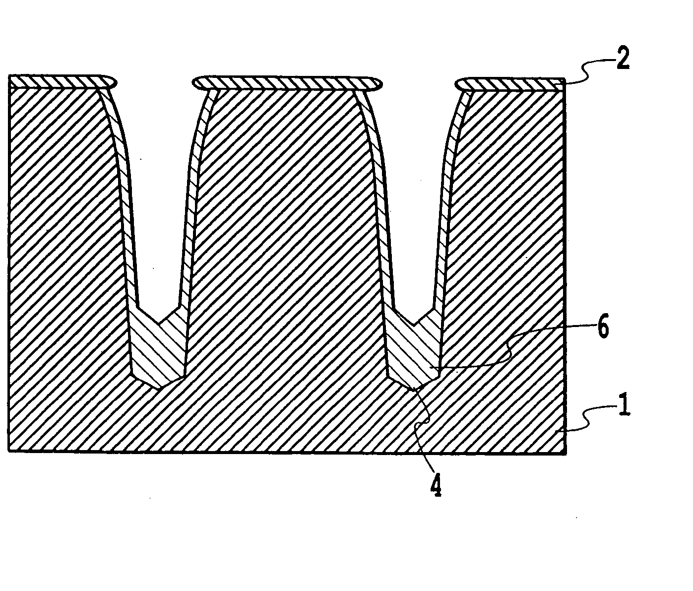
[0036] FIGS. 1-5 are cross-sectional views showing a fabrication process of a semiconductor wafer of an embodiment 1 in accordance with the present invention. First, as shown in FIG. 1, a mask oxide film 2 is formed on a surface of an n-type silicon substrate 1 by thermal oxidation or CVD (Chemical Vapor Deposition). It is also possible to use an insulating film such as a nitride film as the mask besides the oxide film.
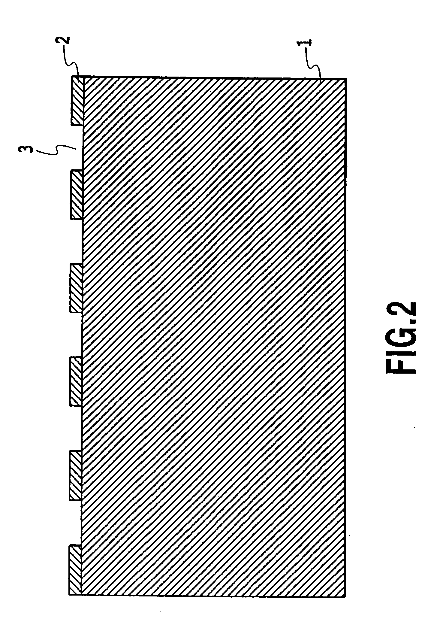
[0037] Subsequently, an alignment target is formed for mask alignment. Then as shown in FIG. 2, windows are formed in the mask oxide film 2 by the photolithography using a mask not shown, thereby forming openings 3 in the mask oxide film 2 for forming trenches. The pattern of the openings 3 can be a stripe-like or lattice-like pattern, or other geometry.
[0038] Subsequently, as shown in FIG. 3, trenches 4 with a desired depth are formed by removing the regions corresponding to the openings 3 from the silicon substrate 1. The trenches 4 are formed by anisotropic plasma ...
embodiment 2
[0054] FIGS. 6 and 7 are cross-sectional views showing a fabrication process of a semiconductor wafer of an embodiment 2 in accordance with the present invention. The embodiment 2 differs from the foregoing embodiment 1 in that when the sidewalls 5 of the trenches 4 consist of the planes, on which facets are formed in the etching process after forming the trenches, the planes are exposed to the sidewalls of the trenches 4 rather than slightly-opening upward the sidewalls of the trenches. As the planes that form facets in the silicon crystal, the (111) plane, (311) plane, (411) plane, (100) plane and the planes equivalent to these planes are known. Thus, the sidewalls 5 of the trenches 4 are made (111) plane, (311) plane, (411) plane, (100) plane and the planes equivalent to these planes. As long as they are planes that enable the facet formation, other plane orientations are possible.
[0055] It is preferable in the embodiment 2 that the etching using the etching gas like HCl proceeds...
embodiment 3
[0061] FIGS. 8-13 are cross-sectional views showing a fabrication method of a semiconductor wafer of an embodiment 3 in accordance with the present invention.
[0062] The embodiment 3 differs from the foregoing embodiments 1 and 2 in the following point. The embodiments 1 and 2 supply the furnace with the growth gas and etching gas at the same time in the epitaxial growth process.
[0063] In contrast with this, the embodiment 3 carries out the epitaxial growth with alternately supplying the growth gas and etching gas to the furnace little by little.
[0064] In the trenches 4 as shown in FIG. 8, facets are formed on its sidewalls 5. Then, the p-type semiconductor 6 is epitaxially grown by supplying the growth gas in the epitaxial growth process without supplying the etching gas. The grown epitaxial film is thick at the bottoms of the trenches 4 and thin on the sidewalls of the trenches 4 as shown in FIG. 9. Subsequently, the etching gas is supplied instead of the growth gas so that the epi...
PUM
 Abstract
Description
Claims
Application Information