Calibration circuit and semiconductor device incorporating the same

a technology of calibration circuit and semiconductor device, applied in logic circuits, line impedence variation compensation, transmission, etc., can solve the problems of increasing the number of driver circuits, unable to enable high-speed data transfer, and still generated noise, so as to achieve stable output levels and stable comparison and judgment

Active Publication Date: 2009-09-29
LONGITUDE LICENSING LTD
View PDF6 Cites 13 Cited by
  • Summary
  • Abstract
  • Description
  • Claims
  • Application Information

AI Technical Summary

Benefits of technology

[0030]The calibration operation of this invention adjusts the impedance after once inactivating transistors of a replica buffer. The impedance adjustment can be realized by configuring such that the level at a calibration pin ZQ and the level at a replica contact point A reach a predetermined potential (VDD / 2) after returning to a ground level and a VDD level, respectively, which are each a constant level. Therefore, it is possible to provide stable output levels at the calibration pin ZQ and the contact point A without being subjected to replica buffer transistor switching noise, thereby achieving an effect that comparators can always carry out stable comparison and judgment.

Problems solved by technology

If the impedance of the transmission line between the semiconductor devices and the output impedance of the semiconductor device are not matched, the data waveform becomes dull during transmission to cause overshoot or undershoot, thereby disabling the high-speed data transfer.
However, although the noise is reduced at the time of switching the state of the group of large transistors, the noise is still generated.
Further, since the number of transistors that should be individually driven increases due to the decimal system, there arises a new problem that the number of driver circuits increases.
However, the foregoing documents each still have a problem that noise is generated at the time of switching the on / off states of the transistors.
In this manner, during the transition period when the control signal is shifted in level, there is a large change in current driving capability and thus a large change in potential occurs as noise.
Accordingly, as shown in FIG. 1, there is a problem that large noise occurs during transition periods when the control signal is shifted in level, thereby disabling accurate calibration.
Therefore, there is the problem that the noise is generated at the time of switching the state of the transistors, thus disabling accurate calibration.

Method used


Image

  • Calibration circuit and semiconductor device incorporating the same
  • Calibration circuit and semiconductor device incorporating the same
  • Calibration circuit and semiconductor device incorporating the same

Examples


Embodiment Construction

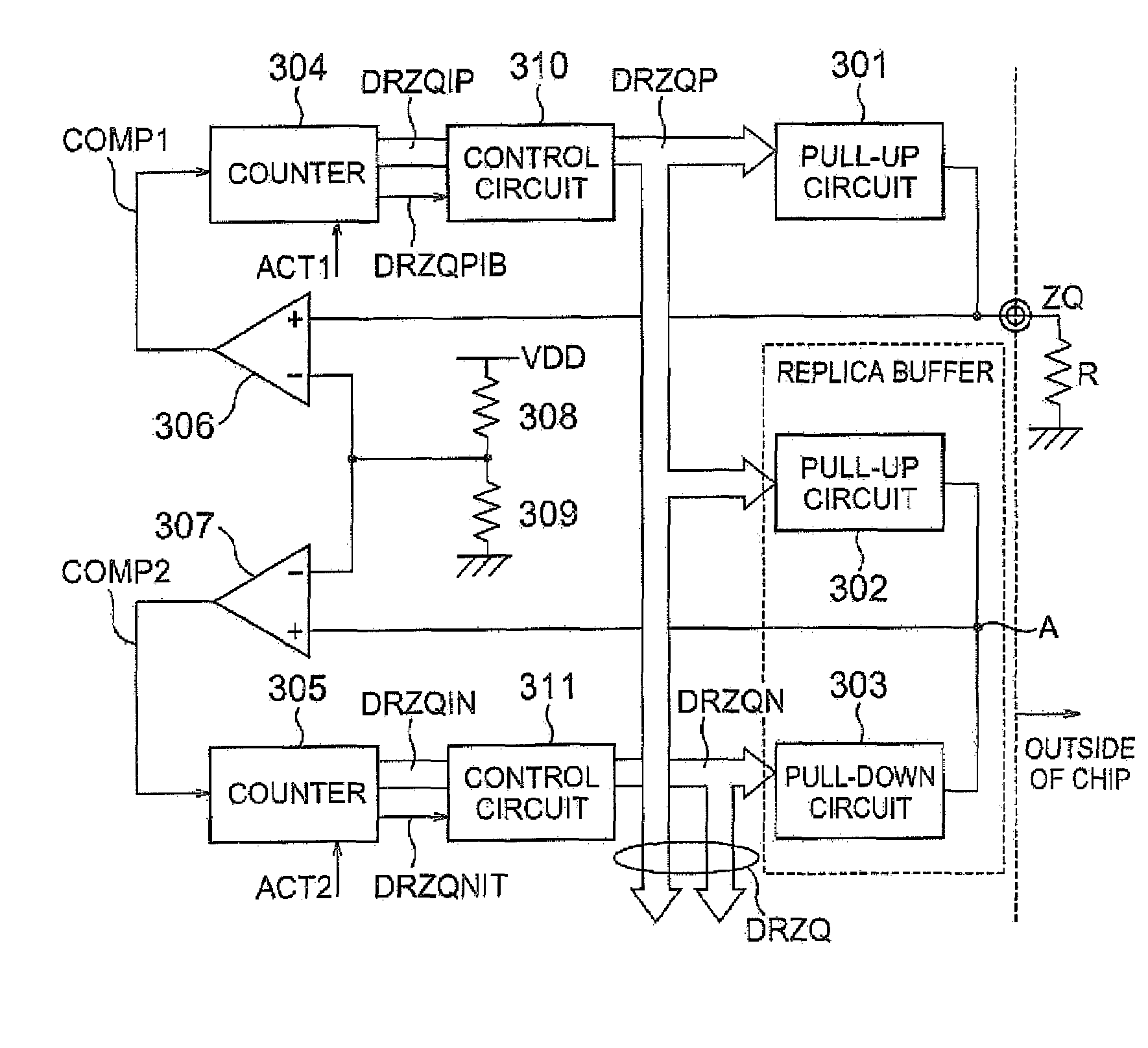
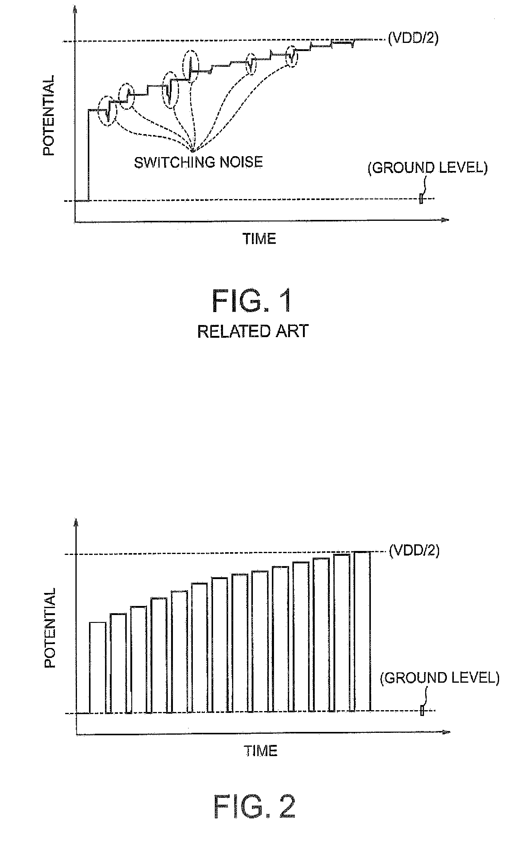
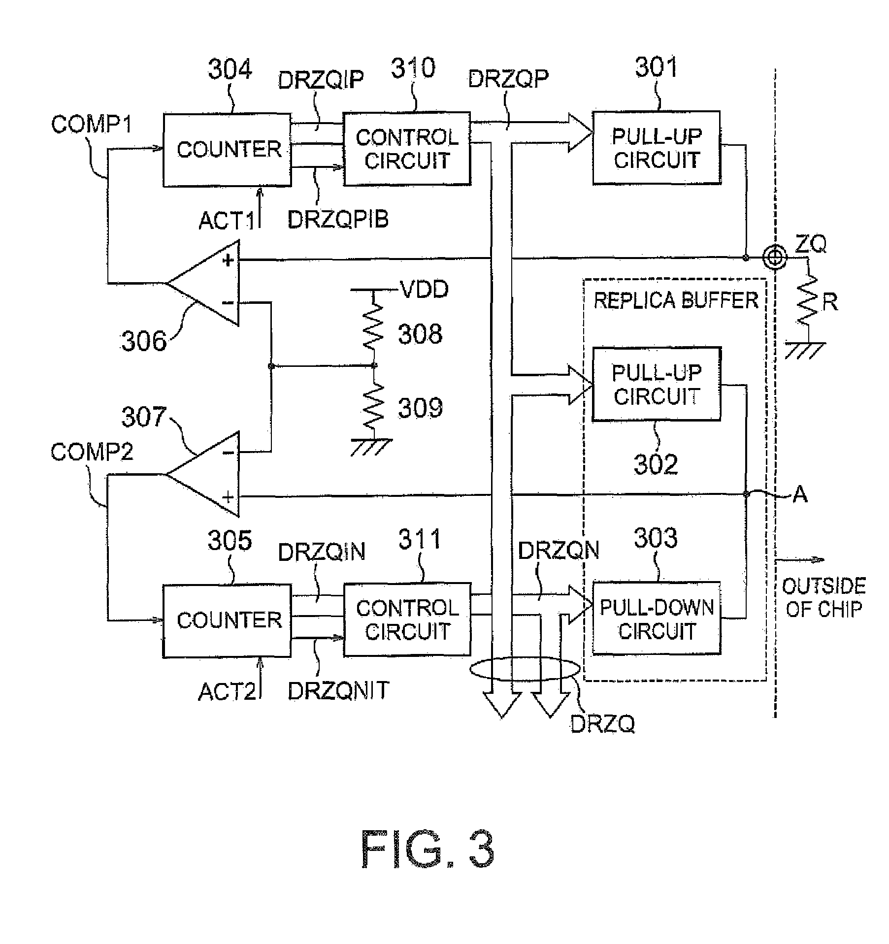
[0040]The best mode of this invention will be described in detail with reference to FIGS. 2 to 9. FIG. 2 shows calibration potential changes in calibration operation according to this invention. The calibration operation of this invention is characterized in that the potential is once returned to an initially set potential and then set to a desired setting potential. FIG. 2 is a diagram showing changes in potential at a calibration contact point in the calibration operation according to this invention. FIG. 3 is a calibration circuit diagram, FIG. 4 is a pull-up circuit diagram, FIG. 5 is a pull-down circuit diagram, FIG. 6 is a pull-up control circuit diagram, and FIG. 7 is a pull-down control circuit diagram. FIG. 8 is a timing chart of calibration operation on the pull-up circuit side and FIG. 9 is a timing chart of calibration operation on the pull-down circuit side.

[0041]A calibration circuit shown in FIG. 3 is incorporated in a semiconductor device and comprises pull-up circui...


PUM


Abstract

Impedance adjusting transistors are once inactivated on every occasion of changing an impedance adjusting code. After restoring the potential to an initially set potential by once inactivating the impedance adjusting transistors, the state of the transistors is switched according to the impedance adjusting code. By starting the potential from the initially set potential at the time of switching the state of the transistors, no switching noise is generated. Since no switching noise is generated, a comparator always carries out stable comparison and judgment and thus there is obtained a calibration circuit that ensures stable outputs.

Description

[0001]This application claims priority to prior Japanese patent application JP 2005-301717, the disclosure of which is incorporated herein by reference.BACKGROUND OF THE INVENTION[0002]1. Field of the Invention[0003]This invention relates to a semiconductor device and, in particular, relates to a calibration circuit adapted for adjusting impedance of an output circuit and to a semiconductor device incorporating such a calibration circuit.[0004]2. Related Art[0005]Recent electronic systems have been speeded up in operation, wherein the data transfer rate between semiconductor devices forming the system has been highly increased. In order to achieve such an ultra high-speed data transfer, a data signal is made to have a small amplitude and, further, the impedance of a transmission line between the semiconductor devices and the output impedance of an output circuit of each semiconductor device are matched together By matching the impedances, the small-amplitude data signal can be trans...

Claims


Application Information

Patent Timeline
Patent Type & Authority Patents(United States)
IPC IPC(8): G01R35/00H03K19/094G11C11/401G11C11/4093H03K19/0175
CPCH04L25/12H04L25/0278
Inventor FUJISAWA, HIROKIYOKO, HIDEYUKI
Owner LONGITUDE LICENSING LTD
Why Eureka
Try Eureka