Semiconductor device
a technology of semiconductors and capacitors, applied in variable capacitors, fixed capacitors, instruments, etc., can solve the problems that the occurrence of power supply resonance caused by external noise nb>2/b> cannot be prevented, and achieve the effect of preventing power supply resonance and preventing the fluctuation of power supply voltag
- Summary
- Abstract
- Description
- Claims
- Application Information
AI Technical Summary
Benefits of technology
Problems solved by technology
Method used
Image

Examples
first embodiment
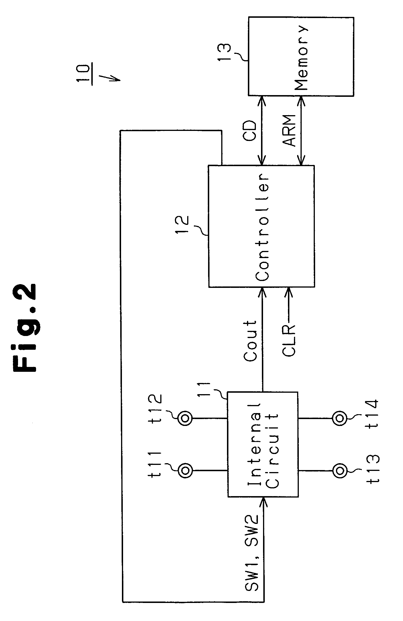
[0032]FIG. 2 is a schematic circuit block diagram of a semiconductor device 10 according to the present invention. The semiconductor device 10 includes an internal circuit 11, a controller 12, and a memory 13. The memory 13 is configured by a non-volatile memory that holds the stored contents even when the supply of power is cut off.
[0033]FIG. 3 shows one example of the internal circuit 11. High potential power supply voltage of, for example., 3 V is supplied to the power supply terminal t11, and ground voltage (0 V) is supplied to the power supply terminal t12 as low potential power supply voltage. The power supply terminals t11 and t12 are respectively connected to a signal processor 15 by power supply wires 14a and 14b (first and second power supply wires) so that the high potential power supply voltage and the low potential power supply voltage are supplied to the signal processor 15.
[0034]The power supply wire 14a includes an inductance L11 and a resistor R11, and the power sup...
second embodiment
[0076]In the second embodiment, the reference voltage (analog voltage) supplied to the comparator 19 may be freely set by adjusting the digital input signal provided to the DA converter 21. Therefore, the reference voltage for determining the occurrence of power supply resonance in the power supply wires 14a and 14b may be set as required.
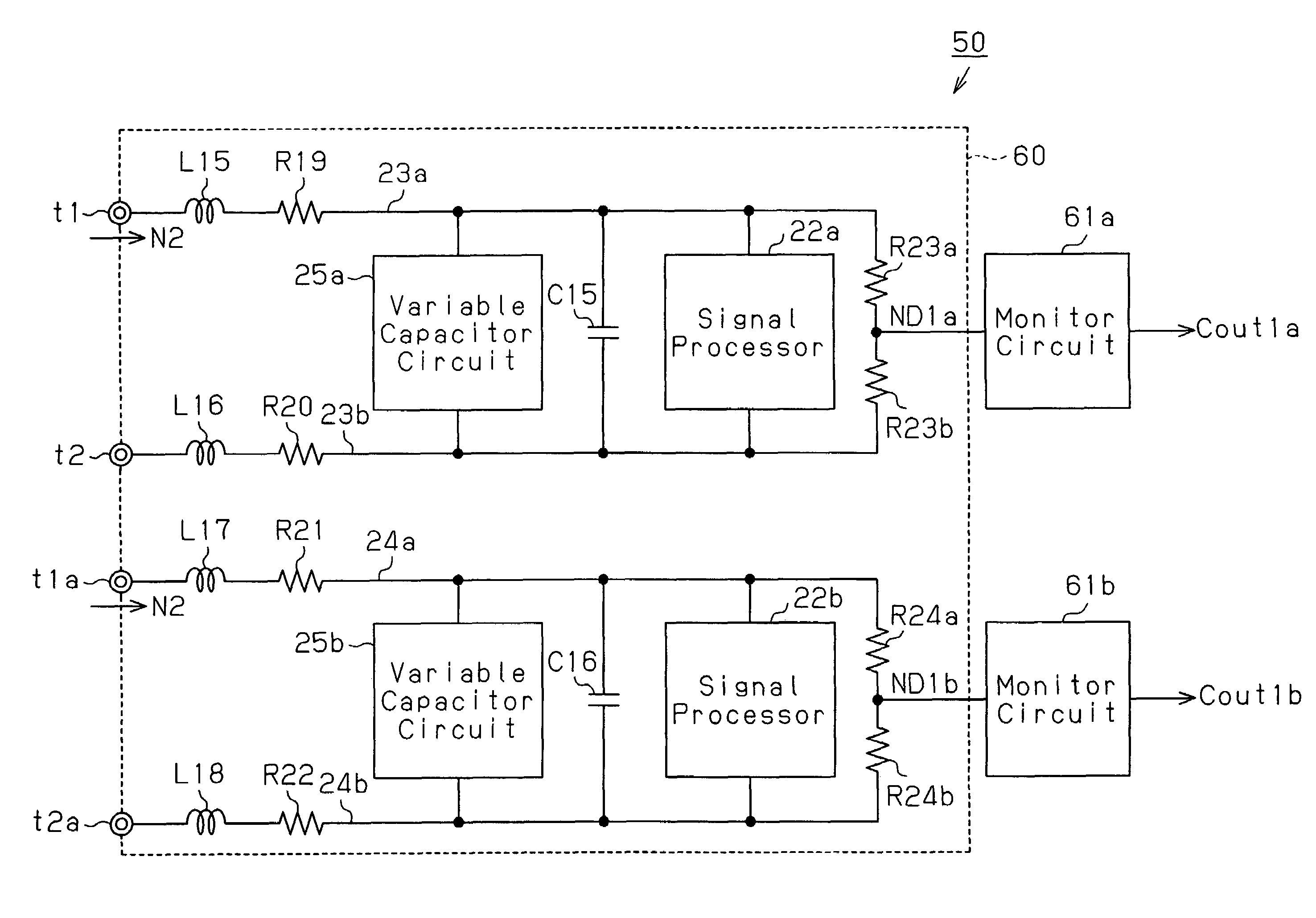
[0077]FIG. 6 is a schematic block circuit diagram of an internal circuit 60 in a semiconductor device 50 according to a third embodiment of the present invention. The internal circuit 60 includes two signal processors 22a and 22b in the third embodiment. Although not shown in FIG. 6, the semiconductor device 50 also includes other components such as the controller 12 and the memory 13 in the same manner as in the first embodiment.
[0078]Power supply voltages (3 V and 0 V) are supplied to the signal processor 22a from power supply terminals t1 and t2 via power supply wires 23a and 23b (first and second power supply wires). The power supply voltages (...
third embodiment
[0082]As a result, in the third embodiment, power supply resonance occurring in the power supply wires 23a and 23b connected to the signal processor 22a is suppressed based on the capacitance value set in the variable capacitor circuit 25a. Further, power supply resonance occurring in the power supply wires 24a and 24b connected to the signal processor 22b is suppressed based on the capacitance value set in the variable capacitor circuit 25b.
[0083]FIG. 7 is a schematic block circuit diagram of an internal circuit 80 in a semiconductor device 70 according to a fourth embodiment of the present invention. In the internal circuit 80 of the fourth embodiment, the variable capacitor circuit 16 of the first embodiment is replaced by a variable capacitor circuit 81. Although not shown in FIG. 7, the internal circuit 80 includes a monitor circuit similar to the monitor circuit 20 of the first embodiment (or the monitor circuit 40 of the second embodiment). The semiconductor device 70 also i...
PUM
 Abstract
Description
Claims
Application Information
 - R&D Engineer
- R&D Manager
- IP Professional
- Industry Leading Data Capabilities
- Powerful AI technology
- Patent DNA Extraction
Browse by: Latest US Patents, China's latest patents, Technical Efficacy Thesaurus, Application Domain, Technology Topic.
© 2024 PatSnap. All rights reserved.Legal|Privacy policy|Modern Slavery Act Transparency Statement|Sitemap