Optical device with raster elements, and illumination system with the optical device

Inactive Publication Date: 2009-10-20
CARL ZEISS SMT GMBH
View PDF28 Cites 24 Cited by
  • Summary
  • Abstract
  • Description
  • Claims
  • Application Information

AI Technical Summary

Benefits of technology

[0016]This had the consequence that in reflective systems of the kind that are used for example in EUV lithography, additional mirrors were required which strongly reduced the light yield of the illumination system. In refractive systems, likewise, a complex high-aperture optical imaging system with a large field has to be used which, for example, includes more than seven individual lenses with aspherical surfaces.
[0017]The invention thus has the objective to propose an optical device, in particular for an illumination system in a microlithographic projection exposure apparatus in which an illuminated area in a field plane of the illumination system can be influenced. Thus, for example, the optical device should allow the illuminated surface to be changed in its position, without the need for a complex and expensive system for the projection of an intermediate field plane in which for example field aperture stops are arranged. The aim is in particular to propose an optical device for an illumination system in which an optical imaging system for producing an image of an intermediate field plane is not necessary, but in which it is possible to influence the illuminated area in the field plane. In particular, by placing the optical device into the light path of an illumination system between a light source and a field plane, the intention is to provide a reflective illumination system in which the field can be influenced, but the light losses are kept as small as possible, for wavelengths ≦100 nm, in particular wavelengths in the EUV range, for example between 5 nm and 30 nm, with preference for 11 nm to 15 nm.
[0021]In an alternative embodiment, a comparable effect can be achieved for a reflective configuration of an optical device with a first optical element with first reflective raster elements and a second optical element with second reflective raster elements, if instead of mutually off-centering a first optical element relative to a second optical element, the second optical element is tilted relative to the first optical element, or if individual second raster elements of the second optical element are tilted. The reflective raster elements are configured as mirrors. By tilting the second raster elements by different tilt angles in a reflective system in which there is generally no longer a common optical axis of the different optical components of the illumination system, the first reflective raster elements can be projected onto different locations in a field plane. This makes it possible to influence the illumination in the field plane and thus to influence the uniformity of the illumination.
[0028]If the aspect ratio differs in the way described above, a crosstalk can be safely avoided. A crosstalk can in particular be safely avoided if the pupil facets have a larger width than the size of the images of the light source that are formed at the location of the pupil facets. For many applications, it is sufficient if the pupil facets are at least made larger in one dimension.
[0029]In an alternative embodiment of the invention, crosstalk can be prevented from occurring, if for example the aspect ratio is the same in field- and pupil facets, through a design where the pupil facets are divided into at least two optical elements arranged one behind the other. The refractive powers of the consecutively arranged optical elements are selected so that they partially compensate each other if the optical axes coincide in one common axis, but that they exhibit a strong prismatic effect when they are laterally offset from each other. This makes it possible in refractive optical devices with field- and pupil facets that have equal aspect ratios or in cylindrical honeycomb plates to shift the illuminated area completely outside of the field range to be imaged, without thereby causing crosstalk to occur.
[0048]In illumination systems for scanning imaging systems, a field aperture stop is arranged preferably away from the field plane in order to create a half-shadowed area at the border of the field and thereby avoid steep jumps in intensity.

Problems solved by technology

The problem presents itself to illuminate this illumination area as homogeneously as possible with the light from the light source.

Method used


Image

  • Optical device with raster elements, and illumination system with the optical device
  • Optical device with raster elements, and illumination system with the optical device
  • Optical device with raster elements, and illumination system with the optical device

Examples


Embodiment Construction

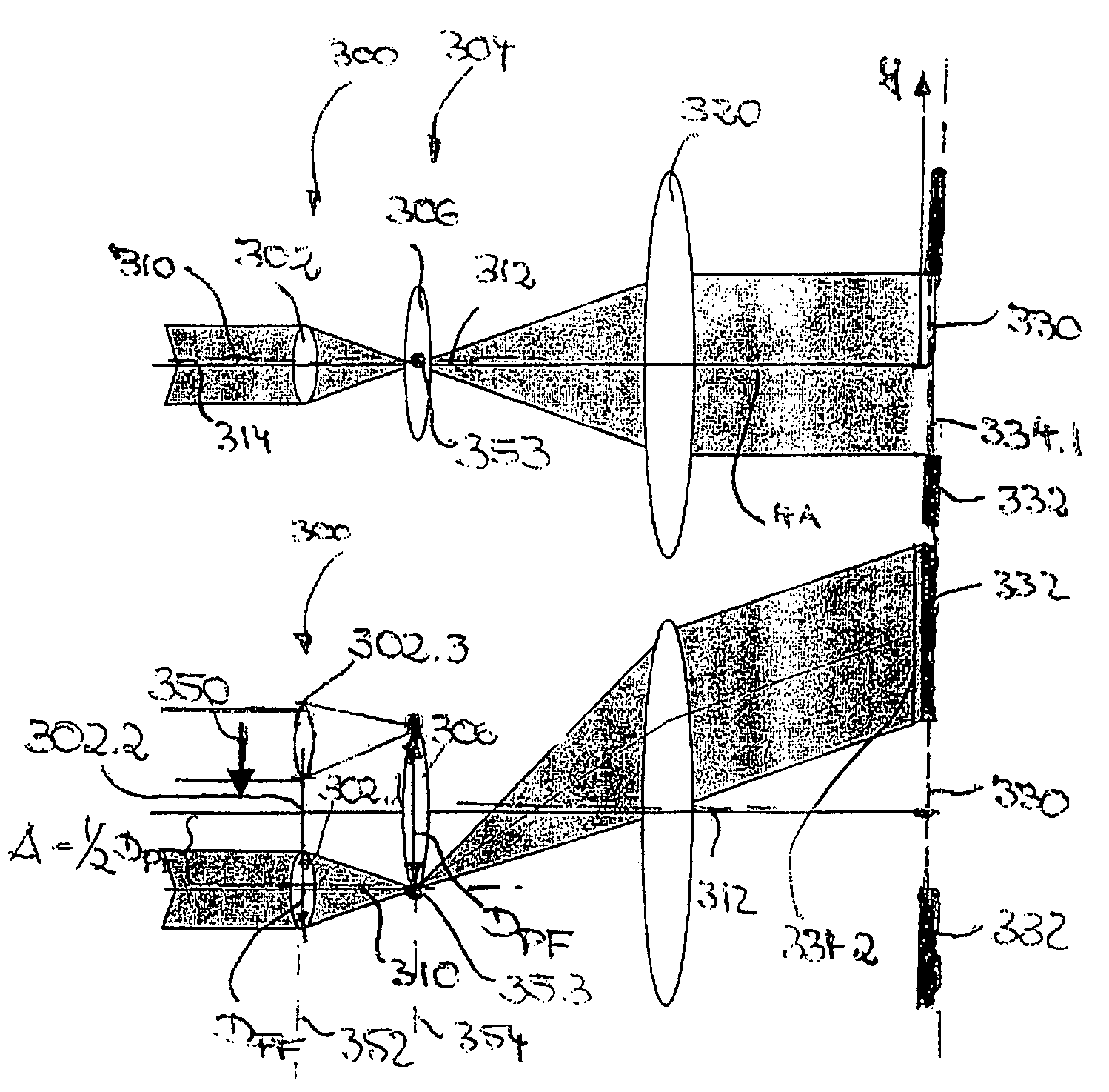
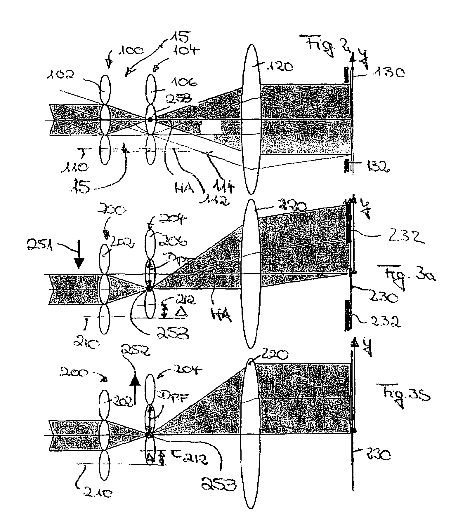
[0014]To delimit the field that is to be illuminated, a variable field aperture stop is always used in state-of-the-art systems.

[0015]These illumination systems suffered from the drawback that to form the projected image of the intermediate field plane in which the variable field aperture stop was arranged, the variable field aperture stop was projected into the reticle plane by means of mirrors or a lens system.

[0016]This had the consequence that in reflective systems of the kind that are used for example in EUV lithography, additional mirrors were required which strongly reduced the light yield of the illumination system. In refractive systems, likewise, a complex high-aperture optical imaging system with a large field has to be used which, for example, includes more than seven individual lenses with aspherical surfaces.

[0017]The invention thus has the objective to propose an optical device, in particular for an illumination system in a microlithographic projection exposure appara...


PUM


Abstract

The invention relates to an optical device that includes (a) a first optical element with at least one first raster element, where the first raster element has a first axis, (b) a second optical element with at least one second raster element, where the second raster element has a second axis. The first raster element can be changed in its position relative to the second raster element, so that a distance between the first axis and the second axis is variable.

Description

CROSS-REFERENCE TO RELATED APPLICATIONS[0001]The present application claims the benefit and priority of the U.S. Provisional Application 60 / 735,659, filed on Nov. 10, 2005. The content of U.S. Provisional Application 60 / 735,659 is incorporated in its entirety in the present application.FIELD OF THE INVENTION[0002]The invention relates to an optical device which is used in particular in an illumination system for microlithographic projection exposure apparatus.[0003]According to a first embodiment, the device includes a first raster element which receives light of a light source, wherein by the first raster element an image of the light source is formed on a second raster element.[0004]According to a second aspect of the invention, the optical device, in particular for an illumination system for use in particular in a microlithographic projection exposure apparatus, includes at least one first optical element with at least one first raster element wherein the first raster element has...

Claims


Application Information

Patent Timeline
Patent Type & Authority Patents(United States)
IPC IPC(8): G03B27/54G03B27/42G21K5/04
CPCG03F7/70075G02B27/0983G02B27/0961G02B17/0657
Inventor SINGER, WOLFGANGWANGLER, JOHANNESDEGUENTHER, MARKUSKUERZ, BIRGITMENKE, CHRISTOPH
Owner CARL ZEISS SMT GMBH
Why Eureka
Try Eureka