Chip LED

a chip led and led light technology, applied in the field of lightemitting diodes, can solve the problems of poor heat dissipation efficiency, and achieve the effects of high power, high light output, and high productivity

Inactive Publication Date: 2012-08-30
E E JAPAN
View PDF7 Cites 19 Cited by
  • Summary
  • Abstract
  • Description
  • Claims
  • Application Information

AI Technical Summary

Benefits of technology

[0015]It is noted, however, that the white color light-emitting chip LED, which is fabricated by sealing the blue color-emitting chip with the epoxy resin containing any phosphor material, presents some problems in which the epoxy resin may be changed to the yellow color when it is exposed to the short wavelength light, and the light output may be decreased.
[0018]It is an object of the present invention to provide a chip LED that eliminates the problems associated with the conventional chip LEDs and described above and can be used for the backlight purposes on the LCD television or lighting.
[0027]The present invention has the advantage in that it is possible to provide a chip LED that can be used for the backlight or lighting purpose on the LCD television.
[0028]In addition, the present invention has the advantage in that it is possible to provide an LED that provides the high power and high light output by taking an advantage of the features of the high productivity and low cost provided by the chip LED.
[0029]Furthermore, the present invention has the advantage in that it is possible to provide an LED module that has the good heat dissipation and the high reliability with respect to the temperature cycle.

Problems solved by technology

The copper foil, which is currently used and includes the copper foil-base metallic layer as well, is so thin (usually 36 μm) that its heat dissipating efficiency is not so good.

Method used


Image

  • Chip LED
  • Chip LED
  • Chip LED

Examples


embodiment

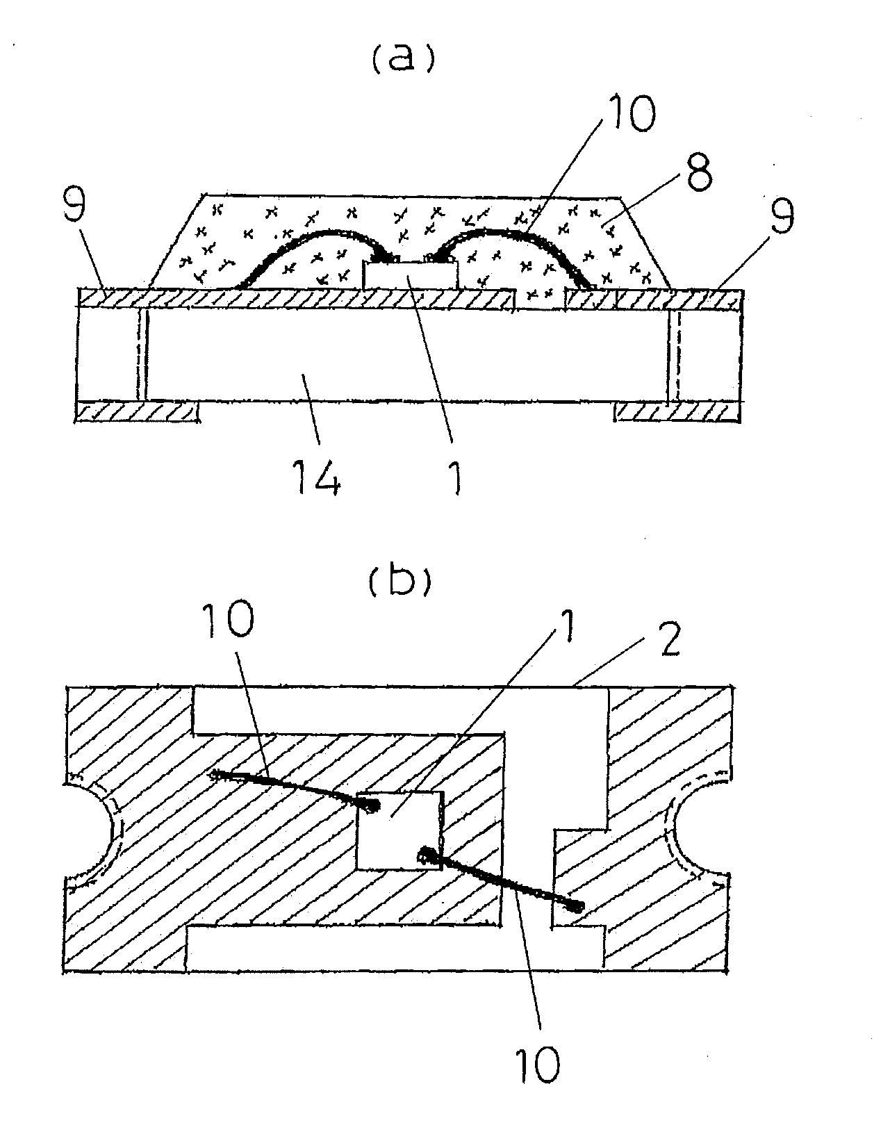
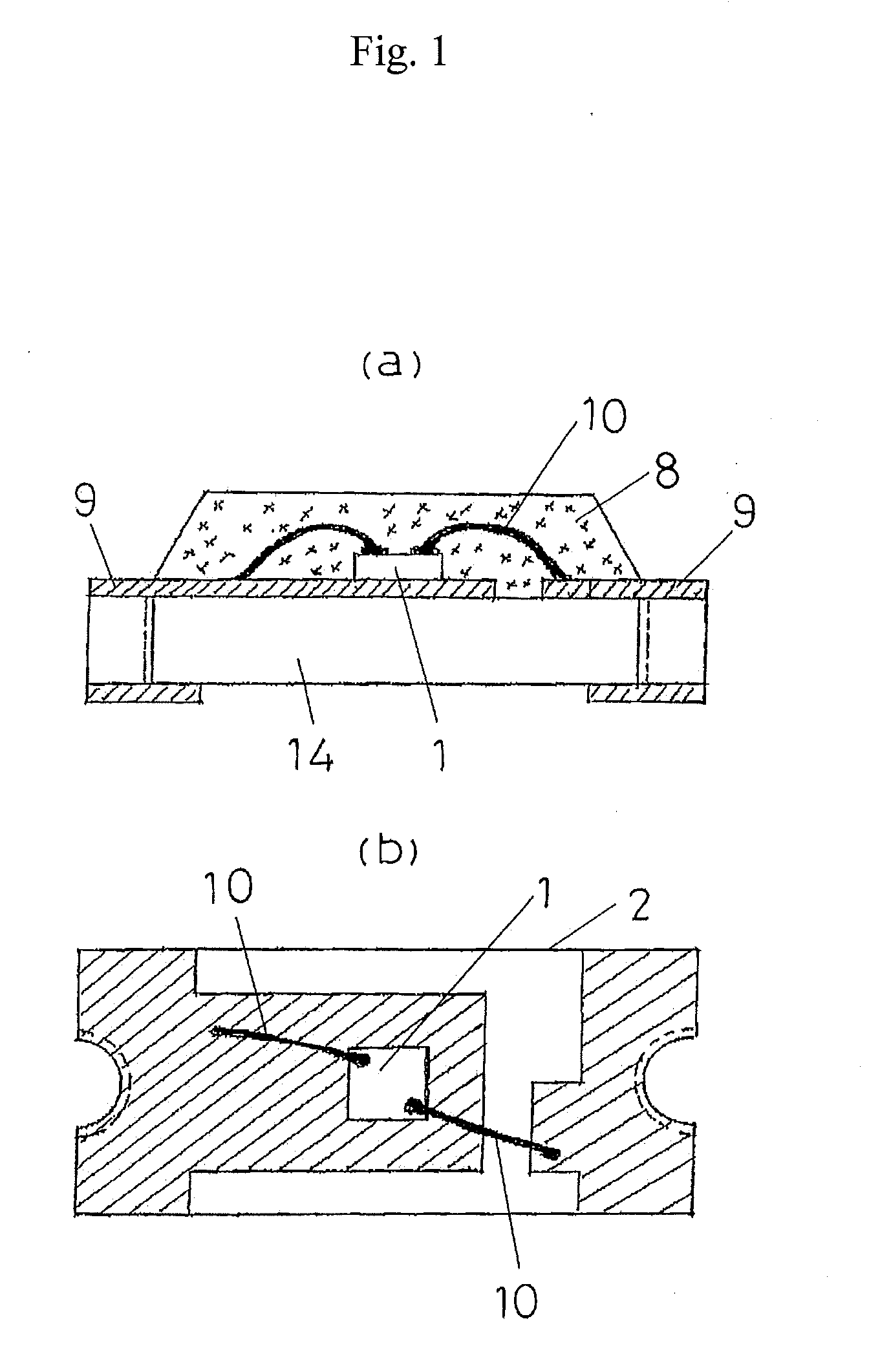
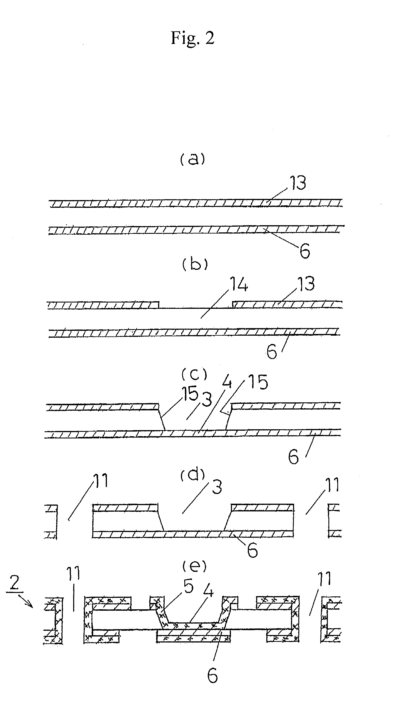
[0051]Similarly to the prior art chip LED, the substrate material 14 which is based on the glass epoxy resin and has the copper foil laminated on both the sides (front side and rear side) thereof may be used (FIG. 2 (a)).

[0052]The copper foil 13 on the side (front side) on which the LED chip 1 is implemented may be bored by the photo-etching process (FIG. 2 (b)).

[0053]The glass epoxy resin-based substrate material 14 that is now bored and exposed may be shaved by the laser beams while the copper foil 13 is masked. The recess 3 may thus be provided (FIG. 2 (c)).

[0054]Considering the light reflectivity of the LED, it is desirable that the recess 3 should have the depth that is greater than the thickness of the LED chip 1 and should be formed to the shape that includes a slant expanding toward the opening on the copper foil 13.

[0055]It is important that the bottom surface 4 of the recess 3 should be extended so that it can reach the copper foil on the rear side of the substrate materia...


PUM


Abstract

The chip LED includes a plurality of semiconductor chips at least one of which is a light-emitting element; a recess formed on the packaging substrate having a rear-side metallic layer on the rear-side thereof, and a metallic layer formed on the bottom surface and inner wall surface of the recess; the light-emitting element being die-bonded to the metallic layer formed on the bottom surface of the recess and being wire-bonded to a wiring pattern deposited on the surface of the packaging substrate; and the metallic layer formed on the bottom surface of the recess being electrically conducted to the rear-side metallic layer formed on the rear side of the packaging substrate.

Description

BACKGROUND OF THE INVENTION[0001]1. Field of the Invention[0002]Generally, the present invention relates to a light-emitting diode (referred to as LED) or any other similar device. More particularly, the present invention relates to the chip LED that employs the glass epoxy resin-based substrate as the packaging or mounting substrate.[0003]2. Description of the Prior Art[0004]The chip LED represents the light-emitting diode that has the high productivity and may be fabricated at low costs. In the conventional prior art, it has been used mainly as the display element that requires less power. In this case, the electric current that flows through those conventional chip LEDs is mostly in the order of 20 mA.[0005]For the recent years and in most cases, this type of LED has been used for the liquid crystal display (LCD) backlight or lighting. It is noted, however, that a relatively large amount of electric current flows through the type of LED that is used for the backlight or lighting ...

Claims


Application Information

Patent Timeline
Patent Type & Authority Applications(United States)
IPC IPC(8): H01L33/40
CPCH01L33/486H01L33/641H01L2224/48091H01L2224/48227H01L2224/48465H01L2224/49113H01L2224/45144H01L2924/00014H01L2924/00
Inventor KUMURA, MASAO
Owner E E JAPAN
Why Eureka
Try Eureka