Electro-optical device and method of manufacturing the same, element driving device and method of manufacturing the same, element substrate, and electronic apparatus

a technology of optical devices and driving devices, applied in the direction of static indicating devices, optics, instruments, etc., can solve the problems of difficult to make the electrical characteristics of the pixel circuits uniform over all pixels, difficulty in reducing and deterioration of display quality. the effect of reducing or avoiding the occurrence of error in the current value of the reference curren

Inactive Publication Date: 2006-11-02
INTELLECTUAL KEYSTONE TECH LLC
View PDF9 Cites 19 Cited by
  • Summary
  • Abstract
  • Description
  • Claims
  • Application Information

AI Technical Summary

Benefits of technology

[0010] In this configuration, the plurality of unit circuits that drive the electro-optical elements are arranged as the IC chips. In characteristics, active elements included in the IC chips have a small variation as compared with thin film transistors made of low-temperature polysilicon. Therefore, even if the number of pixels increases for the purpose of obtaining high precision or large screen of display image, the possibility to generate the variation in characteristics in the unit circuits, which drive the electro-optical elements, can be suppressed. Thus, it is possible to enhance the throughput of the electro-optical device. In addition, since the active elements included in the IC chips are driven with a low voltage compared with the thin film transistor made of low-temperature polysilicon, etc., it is possible to reduce the power consumption by the electro-optical device.
[0070] More preferably, the electronic apparatus includes a first display unit having a light-emitting electro-optical device and a second display unit having a non-emissive electro-optical device. The light-emitting electro-optical device has electro-optical elements emitting light by themselves. A typical example of the light-emitting electro-optical device includes an organic EL display device using the organic EL elements emitting light with brightness corresponding to the supplied current as the electro-optical elements. On the other hand, the non-emissive electro-optical device has the electro-optical elements not emitting light by themselves. A typical example of the non-emissive electro-optical device includes a liquid crystal display device using the liquid crystal in which the transmittance varies correspondingly to the applied voltage as the electro-optical elements. In this electronic apparatus, the light output from the light-emitting electro-optical device reaches the non-emissive electro-optical device to be used for the image display. Therefore, additional lighting devices are not necessary to secure the visibility of display by the non-emissive electro-optical device. Or, even if an illuminating device is provided, the amount of light output from the illuminating device is reduced. In an aspect of this electronic apparatus, the first display unit is rotatably connected to the second display unit through the respective edge portions thereof. According to this aspect, the relative positional relationship between the first display unit and the second display unit can be adjusted, such that the light output from the first display unit efficiently reaches the second display unit.

Problems solved by technology

However, for low-temperature polysilicon, variation in characteristics can easily occur in re-crystallization and, in addition, crystal defects may occur.
Due to such variation and defects, for a display device using thin-film transistors including low-temperature polysilicon, it is very difficult to make the electrical characteristics of the pixel circuits uniform over all pixels.
Thus, the deterioration of the display quality may become more serious.

Method used


Image

  • Electro-optical device and method of manufacturing the same, element driving device and method of manufacturing the same, element substrate, and electronic apparatus
  • Electro-optical device and method of manufacturing the same, element driving device and method of manufacturing the same, element substrate, and electronic apparatus
  • Electro-optical device and method of manufacturing the same, element driving device and method of manufacturing the same, element substrate, and electronic apparatus

Examples


Embodiment Construction

[0125] Now, exemplary embodiments of the present invention will be described with reference to the drawings. Exemplary embodiments described below illustrate an exemplary embodiment of the present invention, are not intended to limit the present invention, and can be modified within the scope of the present invention. In addition, in the respective drawings described hereinafter, the respective elements are illustrated to have sizes that can be recognized in the drawings, and thus the measurements or ratios, etc. of the respective elements may not be to scale.

[0126] A: Configuration of Electro-Optical Device

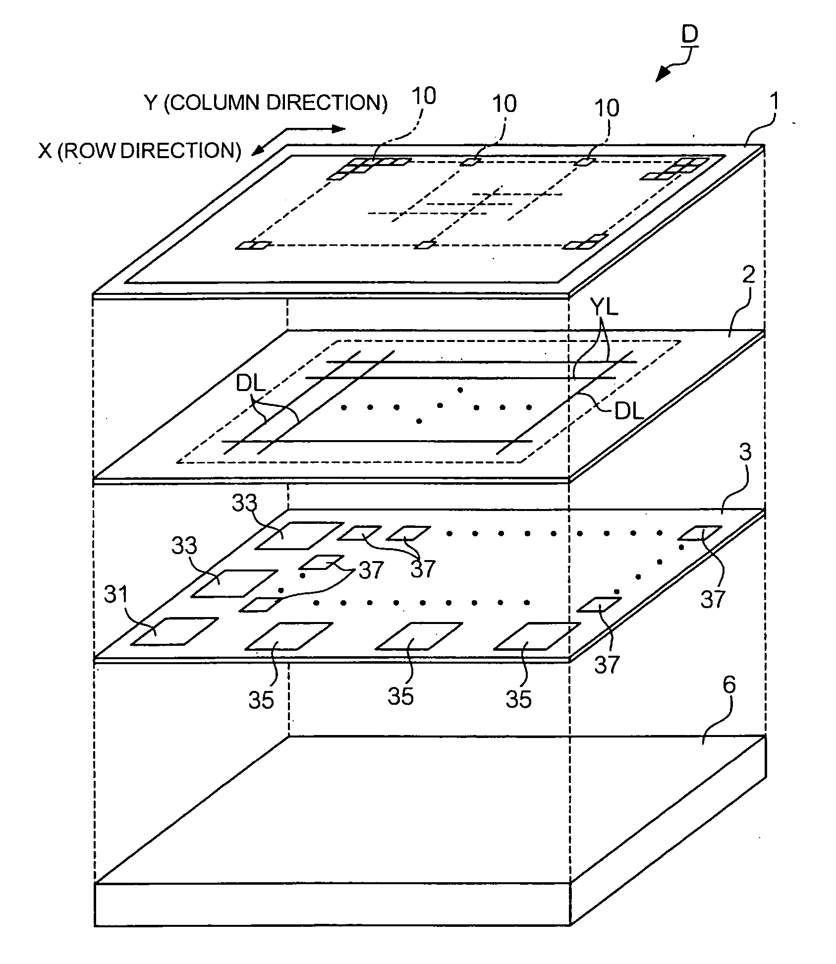
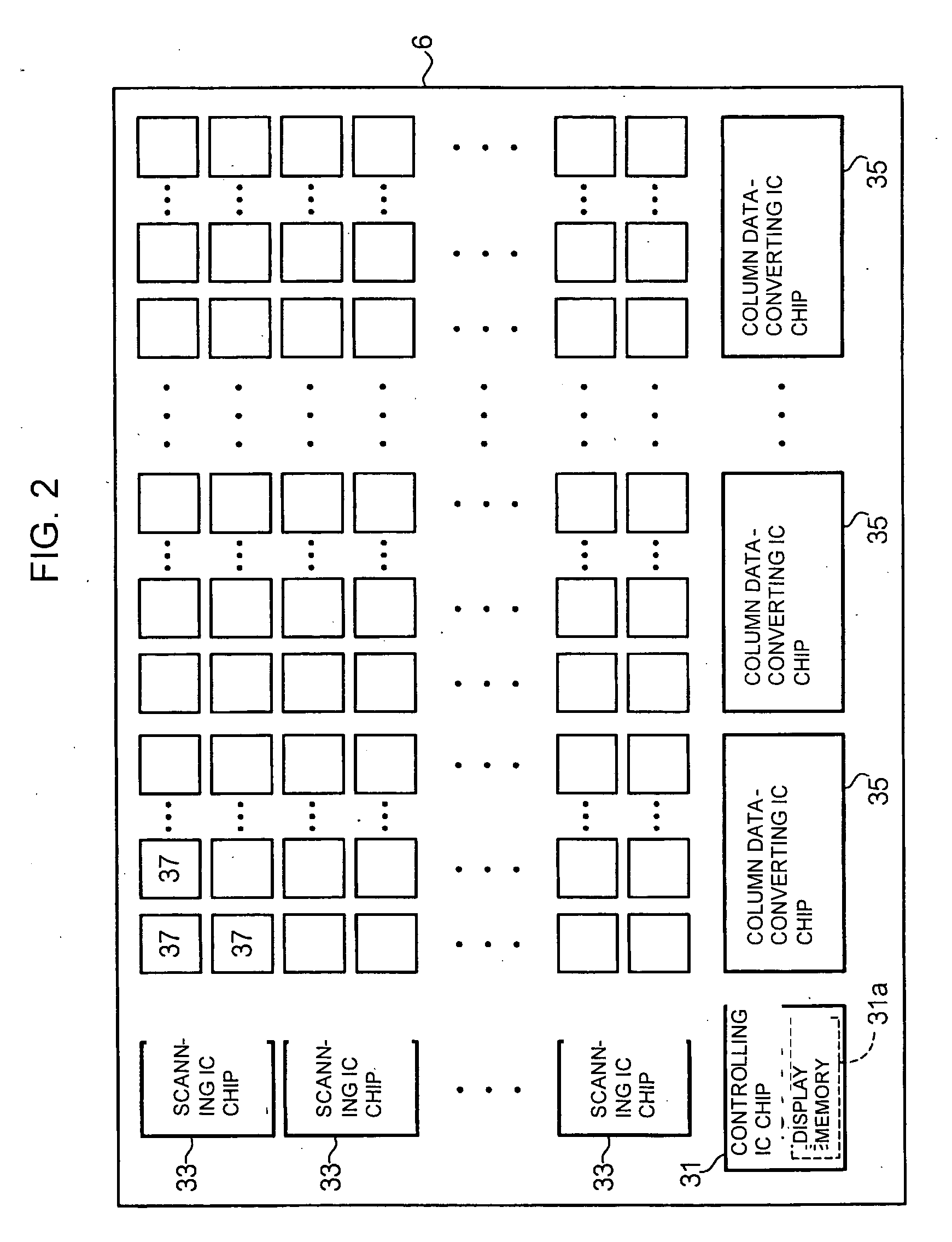
[0127] First, an aspect to which an electro-optical device according to the present invention applies, as a device to display images, will be described. FIG. 1 is a perspective view illustrating an electro-optical device according to an exemplary embodiment of the present invention. As shown in FIG. 1, the electro-optical device D includes a support substrate 6, an organic EL l...


PUM

PropertyMeasurementUnit
widthaaaaaaaaaa
widthaaaaaaaaaa
lengthaaaaaaaaaa

Abstract

In a circuit to drive driven elements such, as electro-optical elements, an electro-optical device has an element layer, a wire-forming layer, and an electronic component layer in order to suppress variation in characteristics of active elements. The element layer has a plurality of organic EL elements, each of which is arranged in a different position in a plane. The electronic component layer has pixel-driving IC chips. The respective pixel-driving IC chips include a plurality of pixel circuits, each of which drives each organic EL element corresponding to the pixel circuit. The wire-forming layer is positioned between the element layer and the electronic component layer. The wire-forming layer has wires to connect the respective pixel circuits included in the pixel-driving IC chips with the organic EL elements corresponding to the pixel circuits.

Description

[0001] This is a Division of application Ser. No. 10 / 445,079 filed May 27, 2003. The disclosure of the prior application is incorporated by reference herein in its entirety.BACKGROUND OF THE INVENTION [0002] 1. Field of Invention [0003] The present invention relates to an element driving device for driving a plurality of driven elements and a method of manufacturing the same, and specifically to an electro-optical device which uses, as the driven elements, electro-optical elements for converting an electrical action into an optical action, and a method of manufacturing the same. In addition, the present invention relates to an element substrate suitable for the element driving device and the electro-optical device, and to an electronic apparatus including the electro-optical device and the element driving device. [0004] 2. Description of Related Art [0005] It has been suggested that electro-optical elements for converting an electrical action into an optical action be used as displa...

Claims


Application Information

Patent Timeline
Patent Type & Authority Applications(United States)
IPC IPC(8): H01L21/00G02F1/1345G06F3/14G09G3/36H01L27/32
CPCG02F1/1345H01L27/3255G06F3/1446H10K59/129H05B33/00G09G3/30G09G3/20
Inventor IMAMURA, YOICHI
Owner INTELLECTUAL KEYSTONE TECH LLC
Why Eureka
Try Eureka