Semiconductor device and designing method for the same

a technology of semiconductor devices and semiconductor elements, applied in the direction of intergral heating, emergency protective arrangements for limiting excess voltage/current, cooking vessels, etc., can solve the problems of difficult to meet the market demand for level 4 strength, the chip area of semiconductor devices is increased or the performance of semiconductor devices is affected, and the device is broken in a second breakdown. achieve good overload tolerance, prevent the increase of manufacturing steps, and improve the effect of electrostatic discharge strength

Inactive Publication Date: 2009-10-20
ABLIC INC
View PDF4 Cites 0 Cited by
  • Summary
  • Abstract
  • Description
  • Claims
  • Application Information

AI Technical Summary

Benefits of technology

[0019]The present invention has been made in view of the points as described above. It is an object of the present invention to provide a semiconductor device including electrostatic discharge protecting means resistant to the air electrostatic discharge without increase in manufacturing cost or degradation in the performance of the semiconductor device.
[0025]In the semiconductor device including the electrostatic discharge protecting means according to the present invention, arranging conductors over the semiconductor circuit consisting of semiconductor devices on the semiconductor substrate causes the application of the electrostatic discharge stress in the air discharge model to the conductors, protecting the application of the electrostatic discharge stress to the semiconductor circuit and permitting the improvement in the electrostatic discharge strength without increase in the chip area or degradation in the performance of the semiconductor device. In the semiconductor device including the electrostatic discharge protecting means according to the present invention, use of the same metal for the wirings as the conductors can prevent the increase in manufacturing steps.
[0026]Further, the conductors are connected to the optimum lines in response to an electrostatic discharge protection capability of the semiconductor device, thus making it possible to constitute a semiconductor device including electrostatic discharge protecting means having a good overload tolerance for the electrostatic discharge.
[0027]Further, connecting the conductors to the optimum lines according to the electrostatic discharge protection capability of the semiconductor device enables the constitution of a semiconductor device including electrostatic discharge protecting means having sufficient electrostatic discharge strength.
[0028]Then, 40% or more of the ratio of the area of the conductors arranged on the semiconductor circuit disposed on a chip (semiconductor substrate) to the area of the chip (semiconductor substrate) can not only provide a semiconductor device including electrostatic discharge protecting means with sufficient efficiency but also permit stable manufacturing of the conductors.
[0029]As described above, according to the present invention a semiconductor device having high-performance electrostatic discharge protecting means can be realized without increase in manufacturing cost.

Problems solved by technology

A semiconductor element such as a transistor included in a semiconductor circuit constituting a semiconductor device is sometimes seriously damaged in an electrostatic discharge event.
The second breakdown starts in the device under the stress as a result of self-heating.
Insufficiency of the methods against the air discharge model, however, makes it difficult to respond to the market demand for Level 4 strength.
Though increase in the area of an electrostatic discharge protection element can resolve the above-described problem, the larger electrostatic discharge protection element and the increase in the area of the chip result in the following problem.
Connection of passive elements such as a resistor, a coil, and a capacitance to the electrostatic discharge protection element can yield higher electrostatic discharge voltage though, resulting not only possible increase in the chip area but also decrease in the CR time constant, which degrade the performance of the semiconductor device.
At this time, a problem occurs that the conventional method can respond to the application of the electrostatic discharge stress to the input / output terminal, but not to the electrostatic discharge stress applied directly to the internal semiconductor circuit 121 of the chip.

Method used


Image

  • Semiconductor device and designing method for the same
  • Semiconductor device and designing method for the same
  • Semiconductor device and designing method for the same

Examples


Embodiment Construction

[0039]A description will be made below of an embodiment of the present invention.

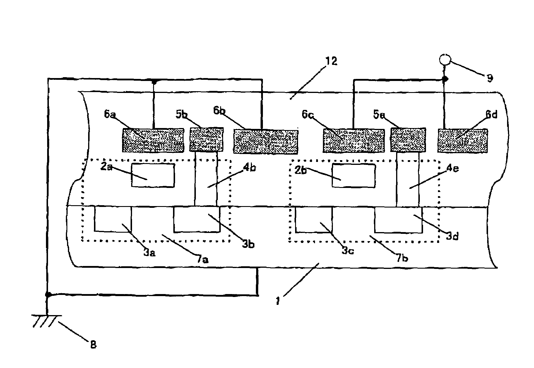
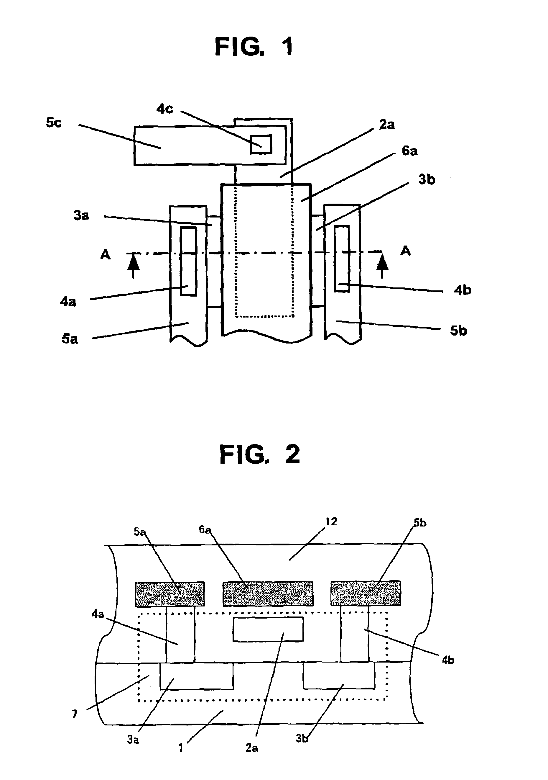
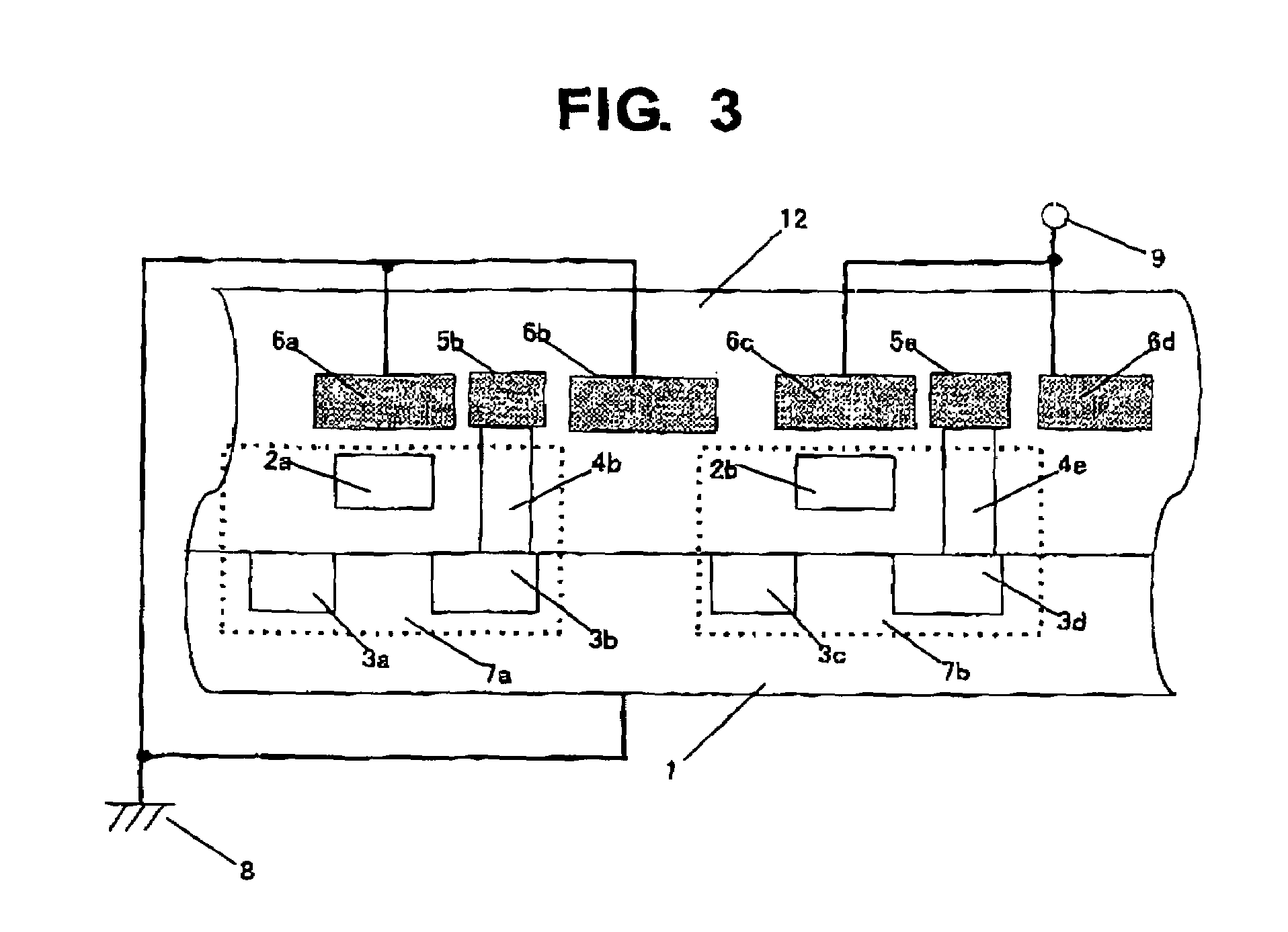
[0040]FIG. 1 is a schematic plan view showing a first embodiment of a semiconductor device including electrostatic discharge protecting means of the present invention. FIG. 2 is a schematic cross-sectional view of the semiconductor device when viewed from a plain indicated by a line A-A shown in FIG. 1. In this drawing, a contact and a wiring which are connected to a gate of a MOS transistor 7 are omitted.

[0041]In FIGS. 1 and 2, a semiconductor device circuit, for example, a MOS transistor 7, is formed on a semiconductor substrate 1 with an impurity concentration in which a resistivity is 1 Ωcm to 20 Ωcm, and the MOS transistor 7 is composed of a diffusion layer 3a serving as a source, a diffusion layer 3b serving as a drain, and polycrystalline silicon 2a serving as a gate. Wirings 5a, 5b, and 5c connected to the diffusion layers 3a and 3b and the polycrystalline silicon 2a are formed of aluminum, for ...


PUM


Abstract

A semiconductor device has a semiconductor circuit provided on a semiconductor substrate. The semiconductor circuit has a source, a drain, a gate and a wiring connected to one of the source, the drain and the gate. Conductors for electrostatic discharge protection are connected to one of a ground line and a power supply line and are disposed over a region of the semiconductor circuit not occupied by the wiring. A ratio of a total area of the conductors disposed over the semiconductor circuit to an area of a chip occupied by the semiconductor circuit is 40% or more.

Description

BACKGROUND OF THE INVENTION[0001]1. Field of the Invention[0002]The present invention relates to a semiconductor device having electrostatic discharge (ESD) protecting means, and more particularly, to a semiconductor device having electrostatic discharge protecting means applied to a CMOS circuit.[0003]2. Description of the Related Art[0004]A semiconductor element such as a transistor included in a semiconductor circuit constituting a semiconductor device is sometimes seriously damaged in an electrostatic discharge event. A main source of an electrostatic discharge exposed to the semiconductor circuit is a human body (“human body model”, abbreviated as HBM), and the discharge from the human body generates current with a peak of several amperes to the semiconductor circuit for about 100 nanoseconds.[0005]The second source of the discharge is a discharge from a metal object (“machine model”, abbreviated as MM), and this source quite possibly induces a transient in which a rise time is...

Claims


Application Information

Patent Timeline
Patent Type & Authority Patents(United States)
IPC IPC(8): H02H3/22
CPCH01L27/0251H01L27/0266A47J27/08A47J27/004A47J36/00A47J43/075
Inventor KOIWA, SUMIO
Owner ABLIC INC
Why Eureka
Try Eureka