
Solid-state image taking apparatus with photoelectric converting and vertical charge transferring sections and method for fabricating the same

a technology of photoelectric conversion and photoelectric pickup, which is applied in the direction of television system scanning details, radioation control devices, television systems, etc., can solve the problems of inability to use, reproducing screen display unevenness, etc., to increase the light receiving area of photodiodes, reduce the area of the vertical ccd channel, and increase the intensity of incident light

Inactive Publication Date: 2009-11-17
SHARP KK
View PDF6 Cites 23 Cited by
  • Summary
  • Abstract
  • Description
  • Claims
  • Application Information

AI Technical Summary

Benefits of technology

[0038]Thus one or more aspect of the invention described herein makes possible the advantages of providing a solid-state image pickup apparatus and a fabrication method thereof which can increase a light receiving area of a photodiode to increase an incident light intensity, and at the same time increase an area of a vertical CCD channel to increase storage amount of signal charge, thereby improving the image quality.
[0041]Therefore, in one or more aspects of the present invention, the vertical CCD channel is located under the photodiode on the side of the semiconductor substrate to arrange the photodiodes and the vertical CCD channel three dimensionally in a direction perpendicular to a semiconductor substrate surface thus, it is not necessary to reduce the area of the vertical CCD channel even when the light receiving area of the photodiode is increased in order to increase the intensity of the incident light to be photoelectric converted. Accordingly, it becomes possible to increase the light receiving area of the photodiodes to increase the incident light intensity to be photoelectric converted, and at the same time, to increase the area of the vertical CCD channel to increase the storage amount of the signal charge. Thus, it becomes possible to aim at improving the image quality of the solid-state image pickup apparatus.
[0042]Specifically, for example, a protruding semiconductor layer of a convex shape is provided on the semiconductor substrate, and a photodiode is provided on an upper surface thereof and the vertical CCD channel on a side wall. In this way, it becomes possible to increase the light receiving area of the photodiodes and increase the area of the vertical CCD channel at the same time. In such a case, it is also possible to increase the area of the vertical CCD channel to further increase the storage amount of the signal charge by further increasing the height of the side wall.
[0043]Further, the photodiodes, the vertical CCD channel and the overflow drain are arranged in a direction perpendicular with respect to the substrate surface. The excess charge is discharged from the overflow drain via the vertical CCD channel. In this structure, compared to the conventional structure where the field shift gate of the vertical CCD channel and the overflow gate are provided on both sides of the photodiode, output unevenness among pixels can be made smaller and a dynamic range can be made broader.
[0045]As described above, the photodiodes as photoelectric conversion sections and the vertical CCD channel as a vertical charge-transferring section are three-dimensionally arranged in a direction perpendicular with respect to the semiconductor substrate surface. Thus, even when the light receiving area of the photodiode is increased in order to increase the light intensity of the incident light to be photoelectric converted, the light receiving area of the photodiodes can be increased to increase the incident light intensity, and at the same time, the area of the vertical CCD channel can be increased to increase the storage amount of the signal charge, without reducing the area of the vertical CCD channel. Accordingly, a solid-state image pickup apparatus with an improved image quality can be obtained.

Problems solved by technology

With such a variance in ranges, display unevenness occurs on a reproduced screen.
Thus, they cannot be used.
As described above, the conventional structure has a problem that display unevenness occurs on a reproduced screen since there is a potential difference A between the field shift gate 110 and the overflow gate 111 for each of the pixels.
Thus, larger light receiving area cannot be secured.
Accordingly, it is difficult to aim at improving image quality by photoelectric converting more incident light hr.
Accordingly, the light intensity of the incident light hr for photoelectric conversion at the photodiode 102 becomes small, and it becomes difficult to aim at improving the image quality.
Thus, it is difficult to aim at improving the image quality of the solid-state image pickup apparatus 100, 120, and 140.
Thus, it was difficult to achieve a good balance between increasing a light receiving area of the photodiode to increase an incident light intensity and increasing an area of the vertical CCD channel to increase the storage amount of a signal charge.

Method used


Image

  • Solid-state image taking apparatus with photoelectric converting and vertical charge transferring sections and method for fabricating the same
  • Solid-state image taking apparatus with photoelectric converting and vertical charge transferring sections and method for fabricating the same
  • Solid-state image taking apparatus with photoelectric converting and vertical charge transferring sections and method for fabricating the same

Examples


Embodiment Construction

[0065]Hereinafter, embodiments of the solid-state image pickup apparatus and fabrication method thereof according to one or more aspects of the present invention will be described with reference to the drawings.

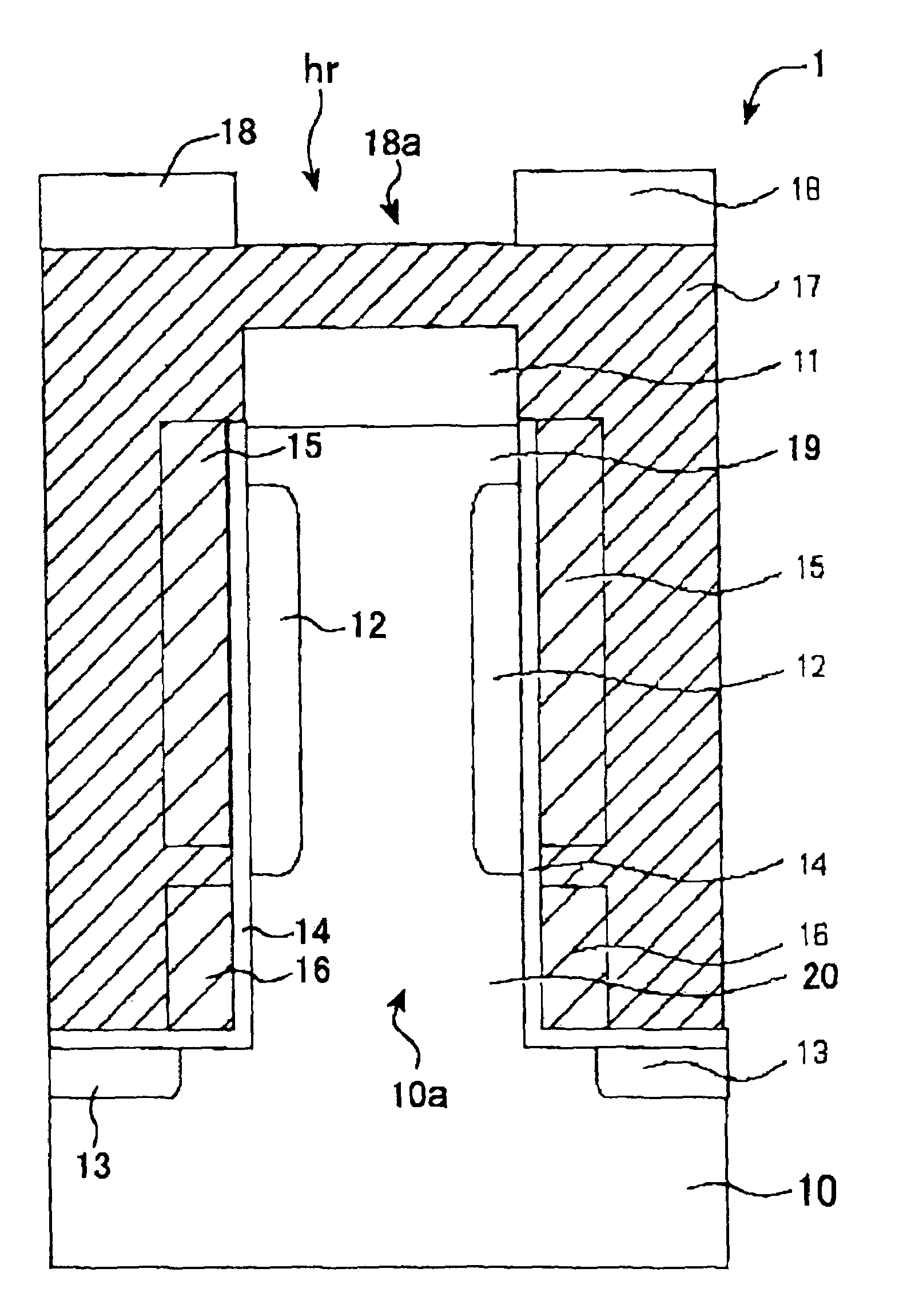
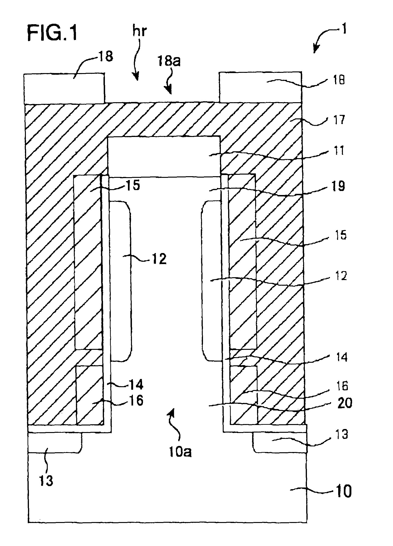
[0066]FIG. 1 is a cross sectional view showing an exemplary structure of one pixel in an embodiment of a solid-state image pickup apparatus. In this embodiment, a p-type silicon (Si) substrate is used for the solid-state image pickup apparatus.

[0067]As shown in FIG. 1, a solid-state image pickup apparatus 1 of this embodiment includes: a protruding semiconductor layer 10a having a convex shape which is provided on a p-type silicon substrate 10 as a semiconductor substrate; and a photodiode 11 which is provided on at least a part of an upper surface of the protruding semiconductor layer 10a as a photoelectric conversion section formed of an n-type diffusion layer.

[0068]Further, a vertical CCD channel 12 as a vertical charge-transferring section is provided on at least apart of...


PUM


Abstract

A solid-state image pickup apparatus includes one or a plurality of photoelectric converting sections for photoelectric converting incident light into a signal charge on a semiconductor substrate, and a vertical charge-transferring section for charge-transferring the signal charge photoelectric converted at the photoelectric converting section, in which the vertical charge-transferring section is located under the photoelectric converting section on the side of the semiconductor substrate.

Description

[0001]This Nonprovisional application claims priority under 35 U.S.C. §119(a) on Patent Application No. 2004-202429 filed in Japan on Jul. 8, 2004, the entire contents of which are hereby incorporated by reference.BACKGROUND [0002]1. Field[0003]The present disclosure relates to a solid-state image pickup apparatus of a Charge Coupled Device (CCD) type which is used as an image taking section of, for example, video cameras and digital still cameras, and a fabrication method for the same, and in particular, to a solid-state image pickup apparatus of a CCD type which is intended to have a higher image quality and a smaller size, and a fabrication method for the same.[0004]2. Description of the Related Art[0005]In recent years, solid-state image pickup apparatuses of CCD type are widely used instead of image pickup tubes since they have characteristics that they are lighter and have longer lives compared to the image pickup tubes. Particularly, recently, such solid-state image pickup ap...

Claims


Application Information

Patent Timeline
Patent Type & Authority Patents(United States)
IPC IPC(8): H04N3/14H04N5/335H01L27/148H04N5/369H04N5/372
CPCH01L27/14656H04N5/335H01L27/14806H01L27/14812H01L27/14687H01L27/14623H04N25/00
Inventor HORII, SHINJI
Owner SHARP KK
Learn More