Conversion apparatus, radiation detecting apparatus, and radiation detecting system

a technology of radiation detection apparatus and conversion apparatus, which is applied in the direction of x/gamma/cosmic radiation measurement, instruments, and radiation controlled devices, etc., can solve the problems of large apparatus, high cost, and complex process of obtaining radioactive ray image data, so as to prevent leakage, suppress noise, and high s/n ratio

Inactive Publication Date: 2009-12-08
CANON KK
View PDF7 Cites 30 Cited by
  • Summary
  • Abstract
  • Description
  • Claims
  • Application Information

AI Technical Summary

Benefits of technology

[0014]The present invention has been made to solve the foregoing problems, and has an object to provide a photoelectric conversion apparatus configured by stacking photoelectric conversion element layers including a photoelectric conversion element over a switching element layer including a switching element, and a radiation detecting apparatus, for preventing leakage caused by an intersection portion between wirings and suppressing noise. Thereby a high S / N ratio can be obtained. Accordingly, image information of high image quality can be obtained.
[0017]According to the present invention, high insulating property is secured at the intersection portion between the signal wiring and the bias wiring outside the pixel region. And thus capacitance between the signal wiring and the bias wiring which becomes parasitic capacitance of the signal wiring is reduced. Whereby noises added to signal charges can be suppressed and an image signal of a high S / N ratio can be obtained. Thus, it is possible to obtain image information of high image quality. Moreover, thick signal wirings can be disposed and wiring resistance of the signal wirings is reduced, whereby it is possible to improve sensitivities of the photoelectric conversion apparatus and the radiation detecting apparatus.

Problems solved by technology

However, in the conventional general radiography, there has been a problem in that a process of obtaining the radioactive ray image is complex.
Thus, there arises a problem in that it takes much time to obtain digitized radioactive ray image data.
However, in the conventional fluoroscopic radiography, there has been a problem in that an apparatus is large-scaled because of use of the electron tube.
The use of the electron tube has created difficulty in obtaining an image having a large area because of a small field of view (detection area).
Furthermore, there has been a problem in that a resolution of an obtained image is low because of the use of the electron tube.
However, as reliabilities at the intersection portions are greatly affected by manufacturing yield or image quality, insulating property is highly required among the wirings.
Thus, the influence of parasitic capacitance or wiring resistance of the signal wiring causes noise of an image signal to be output, creating a possibility of adversely affecting the image signal.
Consequently, it is necessary to secure insulation at the intersection portion of the signal wiring and the drive wiring, and insulation at the intersection portion of the signal wiring and the bias wiring, which cause parasitic capacitance in the signal wiring.
Even when an inorganic material similar to that of the first insulating layer is used for the interlayer insulating layer, its insulation is low due to the low forming temperature.
Furthermore, a reduction in wiring resistance which causes noise in the signal wiring is required.
However, in the FPD configured by arranging the wirings in the matrix, when the wiring is formed large in width, an area at the intersection portion between the wirings becomes large which causes an increase in parasitic capacitance.
However, when the signal wiring is formed thick, it is accompanied by an enlargement of a step.
When the step is enlarged by the signal wiring, it is difficult to uniformly form the interlayer insulating film disposed by covering the signal wiring.
When an inorganic material is used for the interlayer insulating film, it is difficult to form the interlayer insulating film to be thick.
Thus, it is difficult to form the interlayer insulating film which covers a side surface of the signal wiring to be in similar thickness to that of the surface.
In other words, when each wiring is formed thick for the purpose of reducing noise, leakage occurs between the wirings.
Moreover, prevention of leakage leads to insufficient improvement in terms of noise.

Method used


Image

  • Conversion apparatus, radiation detecting apparatus, and radiation detecting system
  • Conversion apparatus, radiation detecting apparatus, and radiation detecting system
  • Conversion apparatus, radiation detecting apparatus, and radiation detecting system

Examples


first embodiment

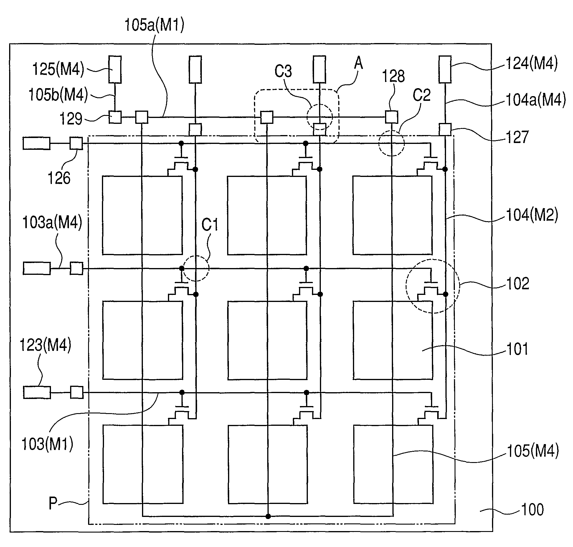
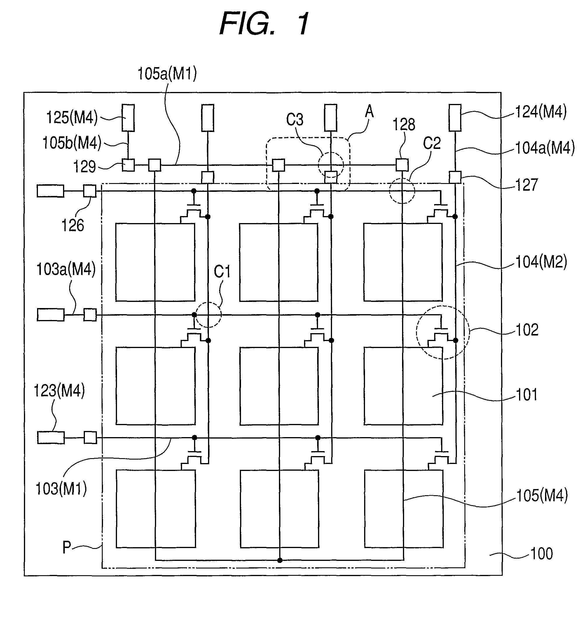
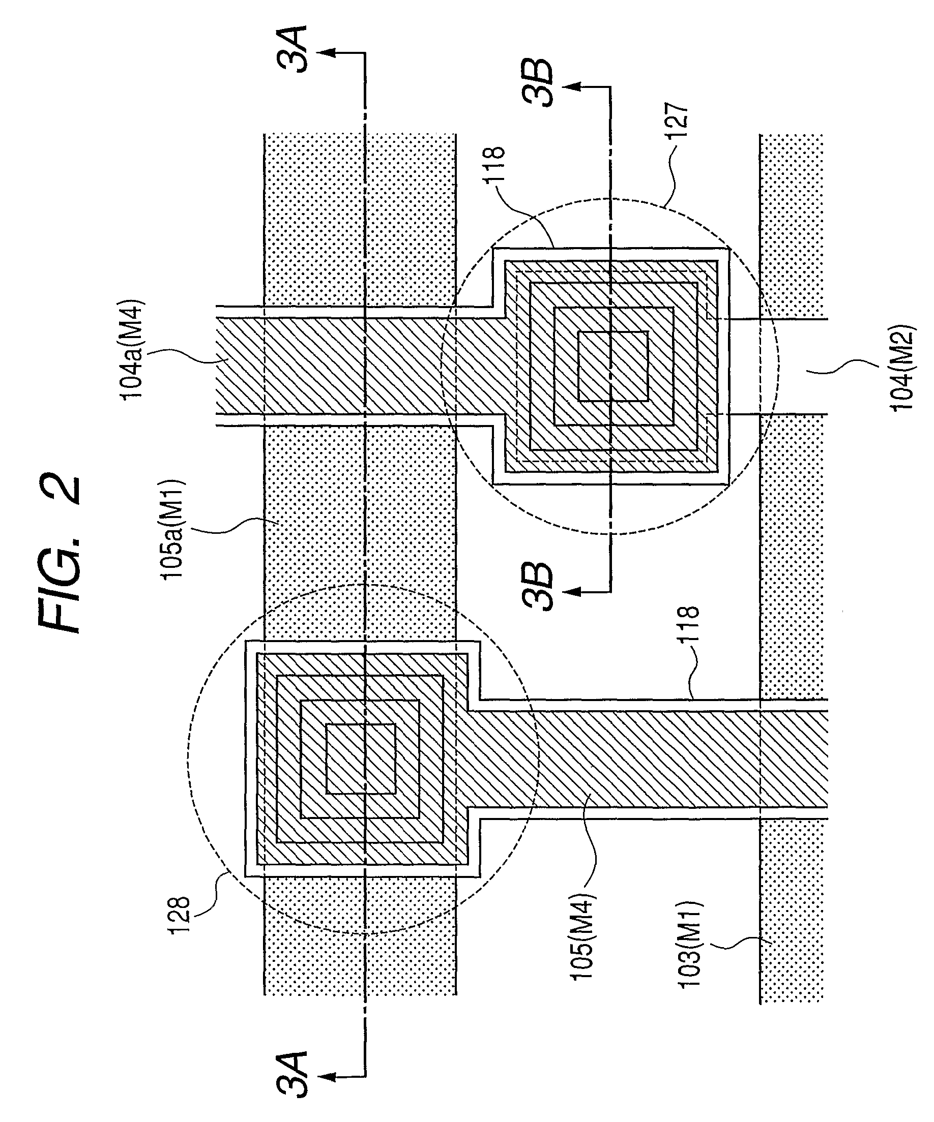
[0033]Referring to FIGS. 1 to 3B, a first embodiment of the present invention will be described in detail. FIG. 1 is a conceptual plan diagram showing a photoelectric conversion apparatus and a radiation detecting apparatus according to the first embodiment of the present invention. FIG. 2 is a conceptual plan diagram of the enlarged area A of FIG. 1. FIG. 3A is a schematic sectional diagram taken on the line 3A-3A of FIG. 2. FIG. 3B is a schematic sectional diagram taken on the line 3B-3B of FIG. 2. In FIGS. 1 to 3B, the same components as those of the conventional FPD shown in FIGS. 10 to 12 will be denoted by the same reference numerals, and detailed description thereof will be omitted.

[0034]In FIGS. 1 to 3B, reference numeral 100 denotes an insulating substrate, 101 a photoelectric conversion element which is a conversion element, 102 a switching element, 103 a drive wiring, 104 a signal wiring, and 105 a bias wiring. For the insulating substrate 100, a glass substrate, a quartz...

second embodiment

[0044]Referring to FIGS. 5 to 6B, a second embodiment of the present invention will be described in detail. FIG. 5 is a conceptual plan diagram in which the area A of FIG. 1 is enlarged. FIG. 6A is a schematic sectional diagram cut on the line 6A-6A of FIG. 5, and FIG. 6B is a schematic sectional diagram cut on the line 6B-6B of FIG. 5. In FIGS. 5 to 6B, components the same as those of the conventional FPD shown in FIGS. 10 to 12, and those of the first embodiment shown in FIGS. 1 to 3B will be denoted by the same reference numerals, and detailed description thereof will be omitted.

[0045]The contact 128 according to the first embodiment is formed via the third metal layer 116 disposed in the one opening on the first bias wiring drawing portion 105a. While the contact 128′ according to the second embodiment is formed via the third metal layer 116 disposed in the two openings on the first bias wiring drawing portion 105a. That is a difference between the first and second embodiments. ...

third embodiment

[0050]Referring to FIGS. 7 to 8B, a third embodiment of the present invention will be described in detail. FIG. 7 is a conceptual plan diagram in which the area A of FIG. 1 is enlarged. FIG. 8A is a schematic sectional diagram cut on the line 8A-8A of FIG. 7, and FIG. 8B is a schematic sectional diagram cut on the line 8B-8B of FIG. 7. In FIGS. 7 to 8B, components the same as those of the conventional FPD shown in FIGS. 10 to 12, those of the first embodiment shown in FIGS. 1 to 3B, and those of the second embodiment shown in FIGS. 5 to 6B will be denoted by the same reference numerals, and detailed description thereof will be omitted.

[0051]According to the second embodiment, the contact 128′ formed via the third metal layer 116 at the two openings on the first bias wiring drawing portion 105a. According to the third embodiment, the contact 128″ is formed via the third metal layer 116 at the opening on the first bias wiring drawing portion 105a and at the opening not on the first bi...


PUM


Abstract

A conversion apparatus of the present invention includes a plurality of pixels including switching elements and conversion elements. The pixels are arranged in a pixel region including a switching element region in which switching elements are arranged in row and column directions and a conversion element region in which conversion elements are arranged in row and column directions. A plurality of wirings are including a second metal layer are connected to the plurality of switching elements of the column direction. Plural bias wirings of a fourth metal layer are connected to plural conversion elements. An external signal wiring of the fourth metal layer outside the pixel region is connected to the signal wirings. An external bias wiring of a first metal layer outside the pixel region is connected to the plurality of bias wirings. The external signal wiring and the external bias wiring intersect each other.

Description

TECHNICAL FIELD[0001]The present invention relates to a conversion apparatus applied to a medical image diagnosis apparatus, a non-destructive inspection apparatus, an analyzer using radioactive rays, or the like, a radiation detecting apparatus using the conversion apparatus, and a radiation detecting system. In the description, electromagnetic waves of visible light or the like, X-rays, α-rays, β-rays, γ-rays, and the like are included in the radioactive rays.BACKGROUND ART[0002]Conventionally, radiography used for medical image diagnosis has been classified into general radiography such as X-ray radiography for obtaining a static image, and fluoroscopic radiography for obtaining a moving image. Each radiography including a imaging apparatus and an image pickup apparatus are selected as occasion demands.[0003]In the conventional general radiography, two systems described below have mainly been implemented. One is a screen film imaging (abbreviated as SF imaging hereinafter) system...

Claims


Application Information

Patent Timeline
Patent Type & Authority Patents(United States)
IPC IPC(8): H01L27/00
CPCH01L27/12H01L27/14603H01L27/14665H01L27/14609H01L27/124
Inventor MOCHIZUKI, CHIORINOMURA, KEIICHIWATANABE, MINORUISHII, TAKAMASA
Owner CANON KK
Why Eureka
Try Eureka