Semiconductor device with electric fuse having a flowing-out region

a technology of electric fuse and semiconductor device, which is applied in the direction of semiconductor device, semiconductor/solid-state device details, radiation control device, etc., can solve the problems of limiting the formation method of insulating film, and the inability to detect the cutting status of electric fuse, so as to improve the cutting condition of electric fuse cu

Active Publication Date: 2009-12-22
RENESAS ELECTRONICS CORP
View PDF7 Cites 15 Cited by
  • Summary
  • Abstract
  • Description
  • Claims
  • Application Information

AI Technical Summary

Benefits of technology

[0017]The present inventor has found a novel technique for cutting electric fuses, in which a constitution of an electric fuse or a manner for applying an electric voltage to an electric fuse is suitably controlled, so that a part of an electric conductor that constitutes an electric fuse is forced to be flowed toward outside of the electric fuse leading to losing a balance between a migration and a supply of the electric conductor material, thereby forming a larger cut part in other part when the electric fuse is cut or broken. This allows maintaining an improved condition in cutting or breaking of a cut electric fuse.
[0018]The electric fuse of the present invention includes a different feature from conventional electric fuses that a “flowing-out region” is formed in the condition after cutting the electric fuse. Here, the term “outside” may be construed as an outside of a region where the second interconnect is formed in the condition before cutting the electric fuse, and may be construed as, for example, an outside of an interconnect trench where the second interconnect is formed. Such configuration allows forming larger void region as a cut part. Further, since the void region is provided in a different location from the location of the flowing-out region, a possibility of a reconnection of the cut electric fuse can be considerably reduced.
[0019]Further, according to the semiconductor device of the present invention, the electric fuse includes a first interconnect, a via coupled to the aforementioned first interconnect and a second interconnect coupled to the aforementioned via, which are formed in different layers, respectively, in the condition before cutting the electric fuse. An excessive electric power is applied to the electric fuse having such configuration, so that a flowing-out region can be formed in an interconnect section having larger area along a direction in the surface of the semiconductor substrate and a void region can be provided in a via section having smaller area along a direction in the surface of the semiconductor substrate. More specifically, by constituting an electric fuse with a connecting structure of interconnects and via, the flowing-out region and the void region can be easily formed. Further, this allows maintaining an improved condition in cutting or breaking of a cut electric fuse.
[0021]Since the electric conductor that constitutes the electric fuse is flowed toward outside from the second interconnect in the condition after cutting the electric fuse according to the method for cutting an electric fuse of the present invention, larger void region can be formed as a cut part. Further, since the void region is provided in a different location from the location where the electric conductor is flowed out, a possibility of a reconnection of the cut electric fuse can be considerably reduced. This allows maintaining an improved condition in cutting or breaking of a cut electric fuse.
[0023]According to the present invention, an improved condition in cutting of a cut electric fuse can be maintained.

Problems solved by technology

Further, it is required to form an insulating film on the hollow portion under a process condition that avoids filling the hollow portion, leading to limiting the formation method of the insulating film.
Further, such fuse element structure may also causes a problem, in which the structure can not be manufactured simultaneously with forming a dual damascene multiple-layered interconnect structure that involves simultaneously forming vias and interconnects.
If such unwanted re-connection is created, an appropriate result of a detection of a cutting status of the electric fuse can not be obtained, even if the electric fuse to be cut is cut once.

Method used


Image

  • Semiconductor device with electric fuse having a flowing-out region
  • Semiconductor device with electric fuse having a flowing-out region
  • Semiconductor device with electric fuse having a flowing-out region

Examples


examples

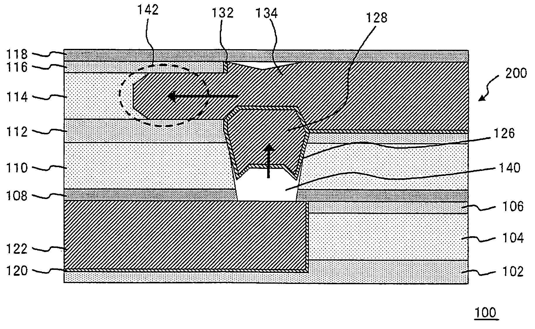
[0091]FIG. 8 shows a cross-sectional view, which was formed by actually forming an electric fuse 200 having an interconnect structure of a single damascene structure similar as shown in FIG. 6A and then cutting the formed fuse via a crack assist type process. Here, an interlayer insulating film, in which the via 128 was formed, was composed of SiOC (Black Diamond, commercially available from Applied Materials Inc., Santa Clara, Calif., USA). Besides, an interlayer insulating film, in which the upper layer interconnect 134 was formed, was composed of SiOC (Aurora, commercially available from ASM International N.V., Holland). Both of the Black Diamond and the Aurora are porous films of SiOC, and the Aurora has lower specific dielectric constant, lower film density and composed of softer film than the Black Diamond.

[0092]As shown in the diagram, in the electric fuse 200, the flowing-out region 142 is formed at the upper layer interconnect 134, and the void region 140 is formed between ...


PUM

PropertyMeasurementUnit
voltageaaaaaaaaaa
widthsaaaaaaaaaa
widthsaaaaaaaaaa

Abstract

A semiconductor device includes an electric fuse formed on a semiconductor substrate and composed of an electric conductor. The electric fuse includes an upper layer interconnect, a via coupled to the upper interconnect and a lower layer interconnect coupled to the via, which are formed in different layers, respectively, in a condition before cutting the electric fuse, and wherein the electric fuse includes a flowing-out region formed of the electric conductor being flowed toward outside from the second interconnect and a void region formed between the first interconnect and the via or in the via, in a condition after cutting the electric fuse.

Description

[0001]This application is based on Japanese patent application No. 2006-130,702, the content of which is incorporated hereinto by reference.BACKGROUND[0002]1. Technical Field[0003]The present invention relates to a semiconductor device and a method for cutting electric fuse, and particularly relates to a semiconductor device including an electric fuse and a method for cutting such electric fuse.[0004]2. Related Art[0005]A technology is conventionally known, in which a fuse is mounted in a semiconductor device, and the electric fuse is broken, so that a value of a resistor employed in the semiconductor device is suitably adjusted, or a failure element is separated and replaced into a normal element.[0006]Typical manner for cutting a fuse includes cutting an electric fuse by irradiating a laser beam in a portion of the fuse and cutting a fuse by applying an electric current.[0007]U.S. Pat. No. 4,064,493, Japanese Laid-open patent publication No. 2005-39,220 and Japanese Laid-open pate...

Claims


Application Information

Patent Timeline
Patent Type & Authority Patents(United States)
IPC IPC(8): H01L29/00H01L21/82
CPCH01L23/5256H01L23/53233H01L23/53238H01L23/53295Y10T29/49107H01L2924/0002H01L27/0288H01L2924/00
Inventor UEDA, TAKEHIRO
Owner RENESAS ELECTRONICS CORP
Why Eureka
Try Eureka