System and method for increasing yield from semiconductor wafer electroplating

a technology of semiconductor wafers and yields, applied in the field of increasing dies, can solve the problems of deformation of solder bumps, adverse effects on the formation of solder bumps, and defects in the form of missing bumps, small bumps, etc., and achieve the effect of reducing the potential for defects on the edge dies

Active Publication Date: 2010-01-05
BELL SEMICON LLC
View PDF2 Cites 92 Cited by
  • Summary
  • Abstract
  • Description
  • Claims
  • Application Information

AI Technical Summary

Benefits of technology

[0008]Through the present invention, a plating ring with a plurality of portions having less than a maximum ring width is provided. With the positioning of the plating ring such that overlap near edge die areas of the semiconductor wafer is avoided, potential for defects on the edge dies is reduced. In this manner, yield loss problems associated with the edge dies are addressed in a straightforward and effective approach.

Problems solved by technology

Such overlapping can adversely affect the plating process.
For example, in flip-chip processing, the formation of the solder bumps is adversely affected, including causing defects in the form of missing bumps, small bumps, and deformed bumps.
As a result of these problems, the affected dies are unusable and yield loss is incurred on every wafer.

Method used


Image

  • System and method for increasing yield from semiconductor wafer electroplating
  • System and method for increasing yield from semiconductor wafer electroplating
  • System and method for increasing yield from semiconductor wafer electroplating

Examples


Embodiment Construction

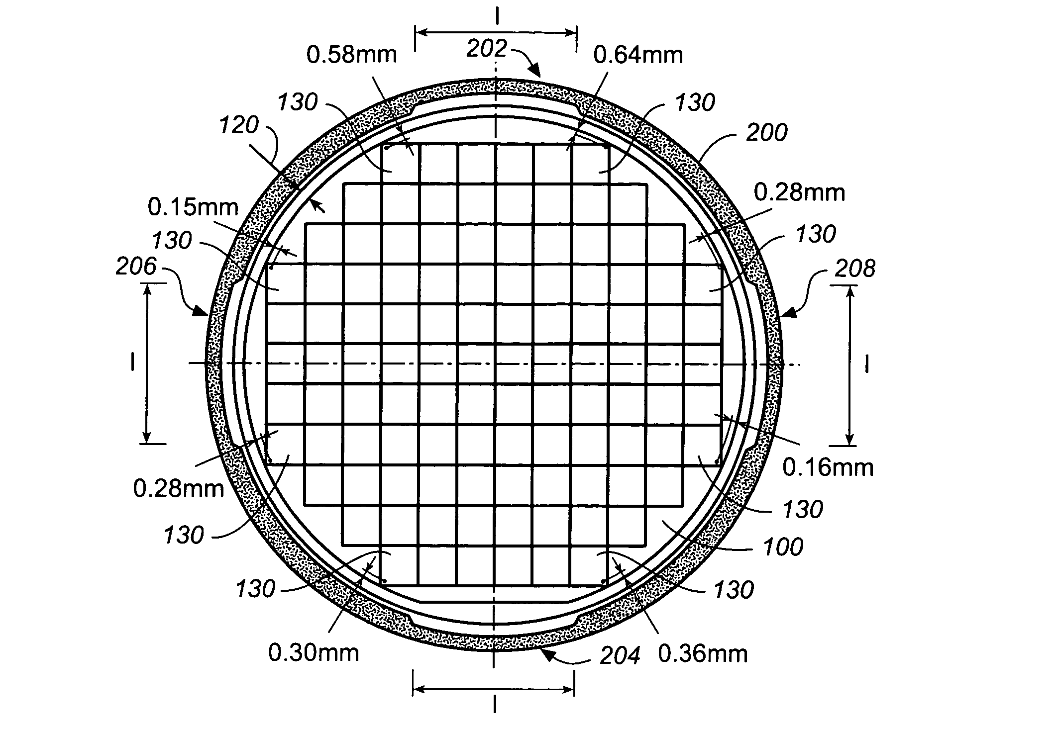
[0013]The present invention relates to increasing die yield from semiconductor wafer electroplating processes. The following description is presented to enable one of ordinary skill in the art to make and use the invention and is provided in the context of a patent application and its requirements. Various modifications to the preferred embodiments and the generic principles and features described herein will be readily apparent to those skilled in the art. Thus, the present invention is not intended to be limited to the embodiments shown, but is to be accorded the widest scope consistent with the principles and features described herein.

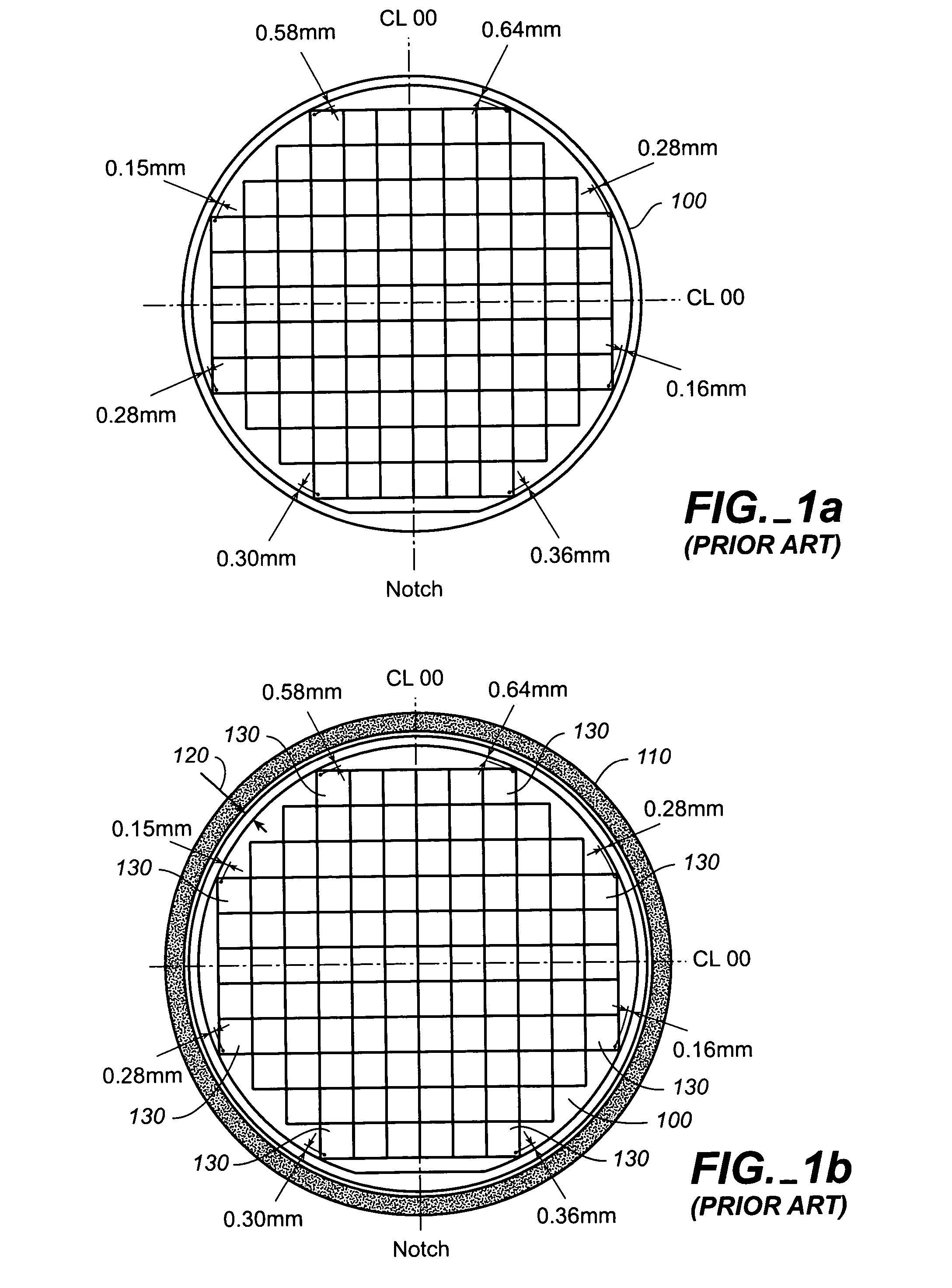
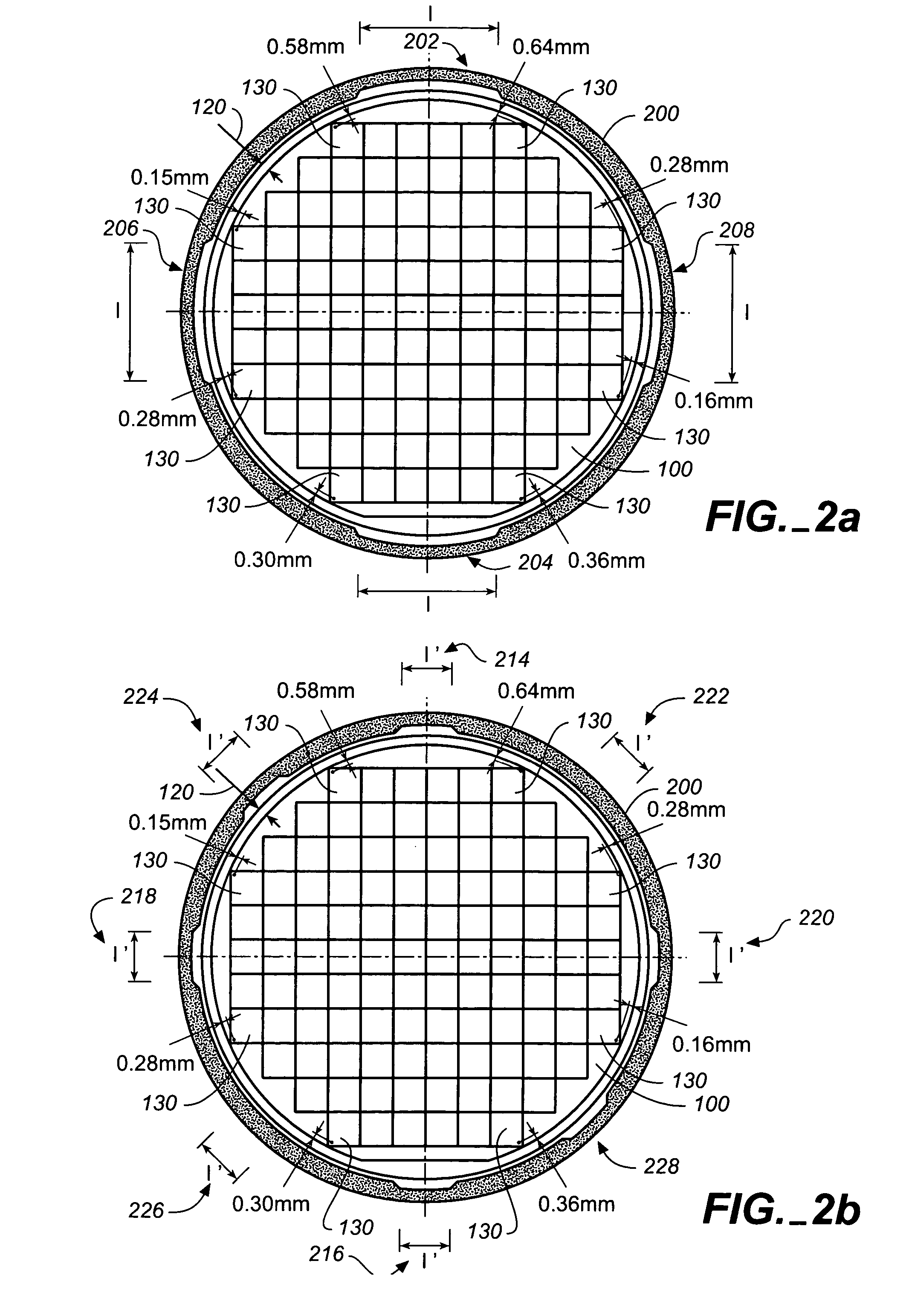
[0014]In accordance with the present invention, a plating ring for use during electroplating processing for wafer bumping is provided that reduces the number of defects in edge dies on the wafer and thus increases yield. In a preferred embodiment, the plating ring of FIG. 1b is altered to reduce the deleterious impact on the dies of the wafer. Typic...


PUM

PropertyMeasurementUnit
widthaaaaaaaaaa
widthaaaaaaaaaa
widthaaaaaaaaaa

Abstract

A system and method increase yield from semiconductor wafer electroplating. The aspects include a semiconductor wafer, the semiconductor wafer comprising a plurality of die areas. A plating ring for holding the semiconductor wafer in position during electroplating is also included, the plating ring substantially surrounding a circumference of the semiconductor wafer and having a width that varies in order to avoid overlap near edge die areas of the semiconductor wafer.

Description

FIELD OF THE INVENTION[0001]The present invention relates to semiconductor wafer electroplating processes, and more particularly to increasing die yield from semiconductor wafer electroplating processes.BACKGROUND OF THE INVENTION[0002]As is commonly understood in the art, the fabrication of microcircuits requires the precise positioning of a number of appropriately doped regions in a semiconductor wafer, followed by effectuation of one or more interconnection patterns. These appropriately doped regions typically include a variety of diffusions and implants, cuts for metallizations and gates, and areas by which connections can be made to bonding pads. For each of these regions a sequence of steps is required, together with a specific pattern layout.[0003]A common method of patterning heretofore has involved a photolithographic transfer followed by etching. As is well known to those skilled in the art, photolithography effects transfer of a desired pattern onto the surface of a silic...

Claims


Application Information

Patent Timeline
Patent Type & Authority Patents(United States)
IPC IPC(8): C25D7/00C25D21/00C25D5/00
CPCC25D7/12C25D17/06H01L21/2885H01L24/11C25D17/001H01L2224/13099H01L2924/0102H01L2924/14H01L2924/01033H01L2924/014H01L2924/00014H01L2924/01078H01L2224/0401H01L2924/00011
Inventor NAGAR, MOHANSHAH, SHIRISH
Owner BELL SEMICON LLC
Why Eureka
Try Eureka