Acceleration sensor

a sensor and acceleration technology, applied in the field of acceleration sensors, can solve the problems of semiconductor acceleration sensors becoming vulnerable to external shocks, thin portions, and sensitizing the acceleration sensor, and achieve the effects of improving shock resistance, thin configuration, and small siz

Inactive Publication Date: 2010-01-26
LAPIS SEMICON CO LTD
View PDF11 Cites 21 Cited by
  • Summary
  • Abstract
  • Description
  • Claims
  • Application Information

AI Technical Summary

Benefits of technology

[0015]It is therefore an object of the present invention to resolve the above-described problems, and to provide an acceleration sensor which can have a small size and thin configuration, and which can have improved shock-resistance.

Problems solved by technology

Normally, when the plummet portion is minimized or made thinner, the moment of inertia becomes smaller, which desensitizes the acceleration sensor.
However, making the beam portion thinner deteriorates the shock-resistance of the semiconductor acceleration sensor, and the semiconductor acceleration sensor may become vulnerable to external shocks, such as shocks caused by dropping.
Moreover, when the beam portion is made thinner, the semiconductor acceleration sensor may be damaged by receiving shocks in its manufacturing process, which can result in a reduction in the yield ratio.
For instance, the semiconductor acceleration sensor may be damaged by water pressure during the dicing process or by force that can be applied to it during pick up.
It is a problem because such process may complicate the overall manufacturing process.
Accordingly, it is a problem because the shock-resistance of the acceleration sensor may be deteriorated due to such arrangement, and the acceleration sensor may become vulnerable to external shocks.

Method used


Image

  • Acceleration sensor
  • Acceleration sensor
  • Acceleration sensor

Examples


first embodiment

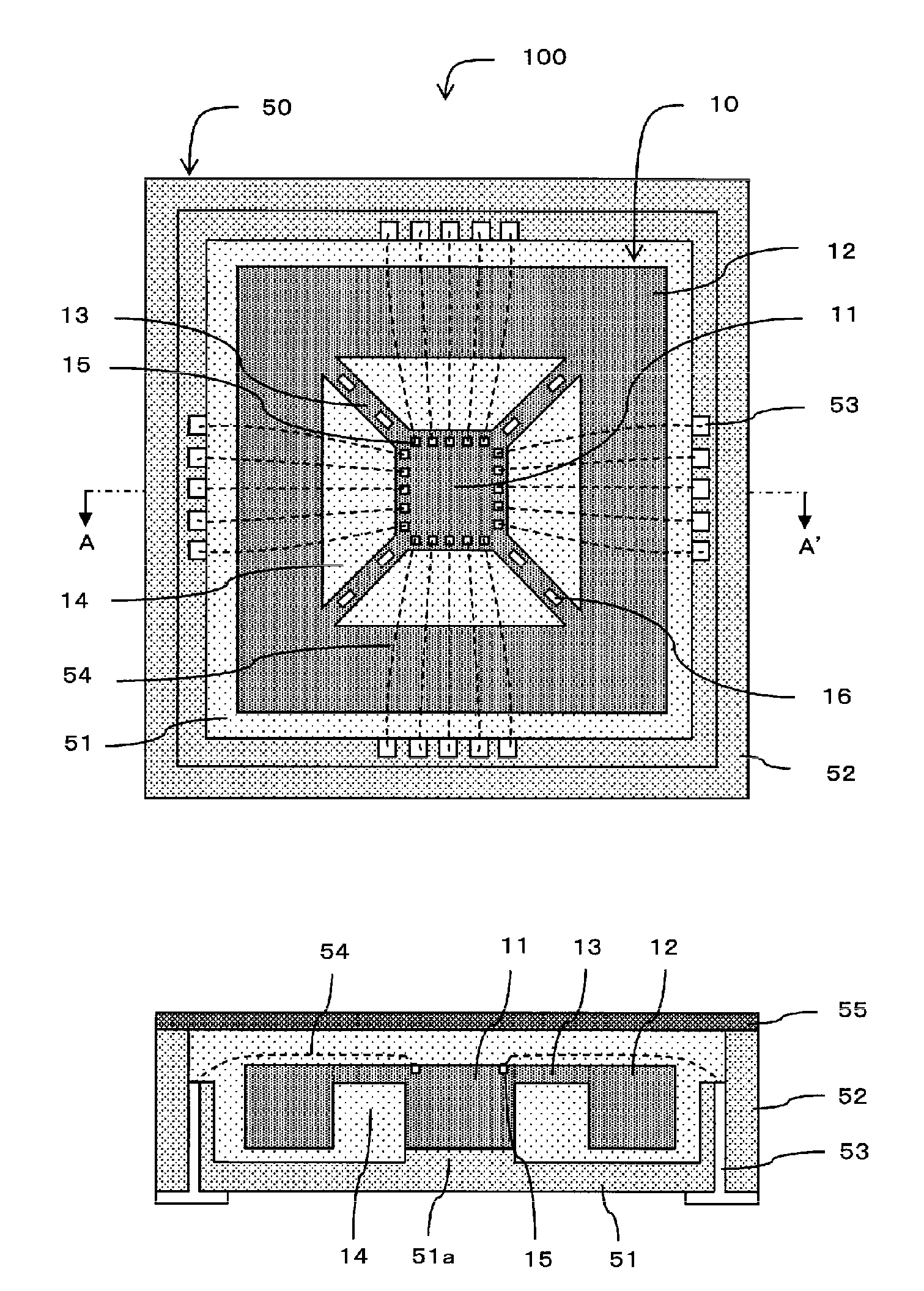
[0026]FIG. 1A and FIG. 1B are diagrams showing the structure of a semiconductor acceleration sensor 100 according to a first embodiment of the present invention. FIG. 1A is a plan view of the semiconductor acceleration sensor 100 when it is viewed from above, and FIG. 1B is a sectional view of the semiconductor acceleration sensor 100 taken along a line A-A′ shown in FIG. 1A. Note that for convenience of explanation, FIG. 1A shows a state in which the cover 55, which is supposed to be placed on the upper surface of the semiconductor acceleration sensor 100, is removed.

[0027]The semiconductor acceleration sensor 100 has a semiconductor acceleration sensor chip 10 housed in a case 50 and it is hermetically sealed by a cover 55.

[0028]The semiconductor acceleration sensor chip 10 is formed using a silicon semiconductor substrate, for instance, and it has a fixed portion 11, a plummet portion 12 and beam portions 13.

[0029]The fixed portion 11 is placed at a central portion of the semicon...

second embodiment

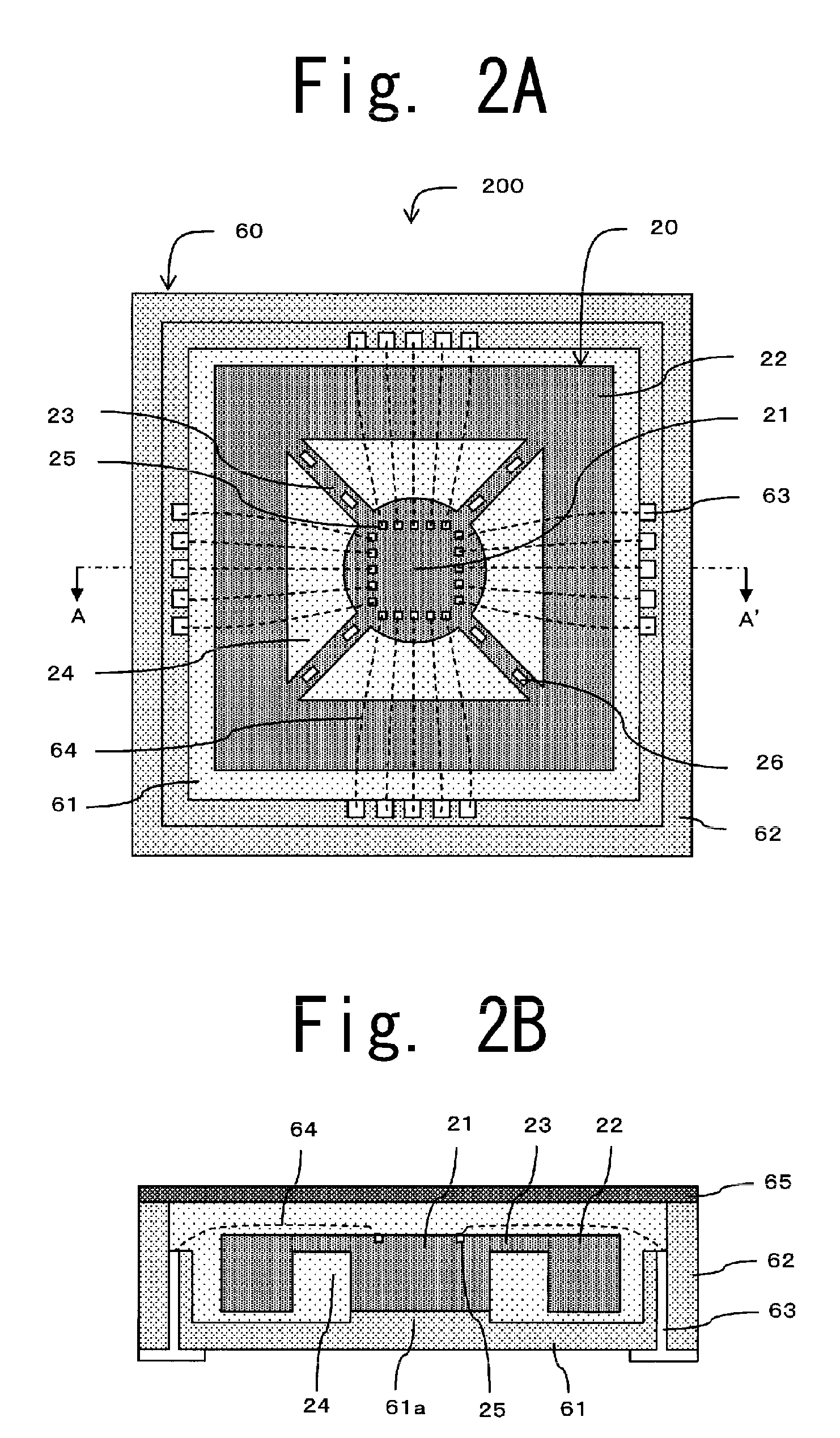
[0041]FIG. 2A and FIG. 2B are diagrams showing the structure of a semiconductor acceleration sensor 200 according to a second embodiment of the present invention. FIG. 2A is a plan view of the semiconductor acceleration sensor 200 when it is viewed from above, and FIG. 2B is a sectional view of the semiconductor acceleration sensor 200 taken along a line A-A′ shown in FIG. 2A. Note that for convenience of explanation, FIG. 2A shows a state in which a cover 65, which is supposed to be placed on the upper surface of the semiconductor acceleration sensor 200, is removed.

[0042]The semiconductor acceleration sensor 200 has a semiconductor acceleration sensor chip 20 housed in a case 60 and it is hermetically sealed by the cover 65.

[0043]The semiconductor acceleration sensor chip 20 is formed using a silicon semiconductor substrate, for instance, and it has a fixed portion 21, a plummet portion 22 and beam portions 23.

[0044]The fixed portion 21 is placed at a central portion of the semico...

third embodiment

[0058]FIG. 4A and FIG. 4B are diagrams showing the structure of a semiconductor acceleration sensor 300 according to a third embodiment of the present invention. FIG. 4A is a plan view of the semiconductor acceleration sensor 300 when it is viewed from above, and FIG. 4B is a sectional view of the semiconductor acceleration sensor 300 taken along a line A-A′ shown in FIG. 4A. Note that for convenience of explanation, FIG. 4A shows a state in which a cover 75, which is supposed to be placed on the upper surface of the semiconductor acceleration sensor 300, is removed.

[0059]The semiconductor acceleration sensor 300 has a structure in which a semiconductor acceleration sensor chip 10 or 20 is mounted on an integrated circuit 30 which controls the semiconductor acceleration sensor chip 10 or 20, and is housed in a case 70 together with the integrated circuit 30 which is hermetically sealed by the cover 75.

[0060]In this embodiment, both the semiconductor acceleration sensor chip 10 accor...


PUM


Abstract

An acceleration sensor has a semiconductor acceleration sensor chip and a case. The semiconductor acceleration sensor chip has a fixed portion, a plummet portion surrounding the fixed portion without contacting the fixed portion, and a beam portion connecting the fixed portion and the plummet portion, the thickness of the beam portion being thinner than the thickness of the fixed portion. The case has a cavity housing the semiconductor acceleration sensor chip, and a projection portion formed on the bottom face of the cavity, the bottom face of the fixed portion being fixed to the top face of the projection portion.

Description

BACKGROUND OF THE INVENTION[0001]1. Field of the Invention[0002]The present invention relates to an acceleration sensor, which in particular is capable of detecting accelerations acting upon three axes, respectively.[0003]2. Background Information[0004]In recent years, acceleration sensors are widely used in all kinds of precision instruments, cars, robots and other various industrial fields. Especially, there is an increasing demand for a semiconductor acceleration sensor, which uses an MEMS (micro electro mechanical system) technology, as it is small in size, light, accurate and reliable in operation, and available at low cost.[0005]In most semiconductor acceleration sensors, the piezoresistance effect, i.e. a phenomenon in which an electric resistivity changes in proportion to stress, is used in detecting acceleration. A common semiconductor acceleration sensor, for instance, is formed by having a semiconductor acceleration sensor chip fixed on a pedestal of a ceramic substrate f...

Claims


Application Information

Patent Timeline
Patent Type & Authority Patents(United States)
IPC IPC(8): G01P15/12G01P15/08G01P15/18H01L29/84
CPCG01P1/023G01P15/18G01P15/123G01P2015/084H01L2224/45144H01L2924/1461H01L2224/49171H01L2224/48227H01L2224/48137H01L2224/48091H01L2924/00014H01L2924/00
Inventor INO, YOSHIHIKO
Owner LAPIS SEMICON CO LTD
Why Eureka
Try Eureka