Output buffer circuit

a buffer circuit and output technology, applied in the field of output buffer circuits, can solve the problems of change in output delay and increase in delay, and achieve the effect of reducing output delay

Active Publication Date: 2010-02-02
RENESAS ELECTRONICS CORP
View PDF13 Cites 6 Cited by
  • Summary
  • Abstract
  • Description
  • Claims
  • Application Information

AI Technical Summary

Benefits of technology

[0011]The present invention has an object to provide an output buffer circuit capable of reducing an output delay.
[0013]A switching speed of the driver signal can be increased, thereby reducing an output delay.

Problems solved by technology

The operation of the constant current source therefore takes time, sometimes causing an increase in delay.
In addition, the signals having a long “L” period and a long “H” period input to the input node vi cause a change in output delay.

Method used


Image

  • Output buffer circuit
  • Output buffer circuit
  • Output buffer circuit

Examples


first preferred embodiment

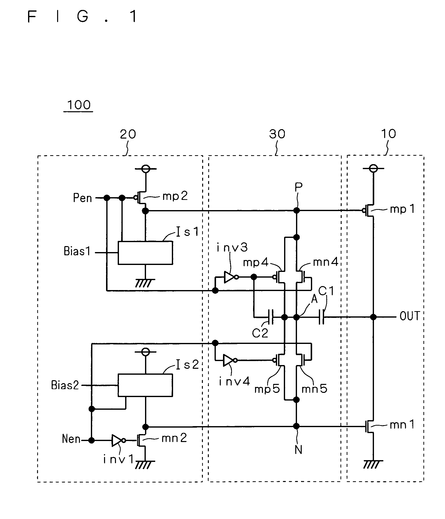
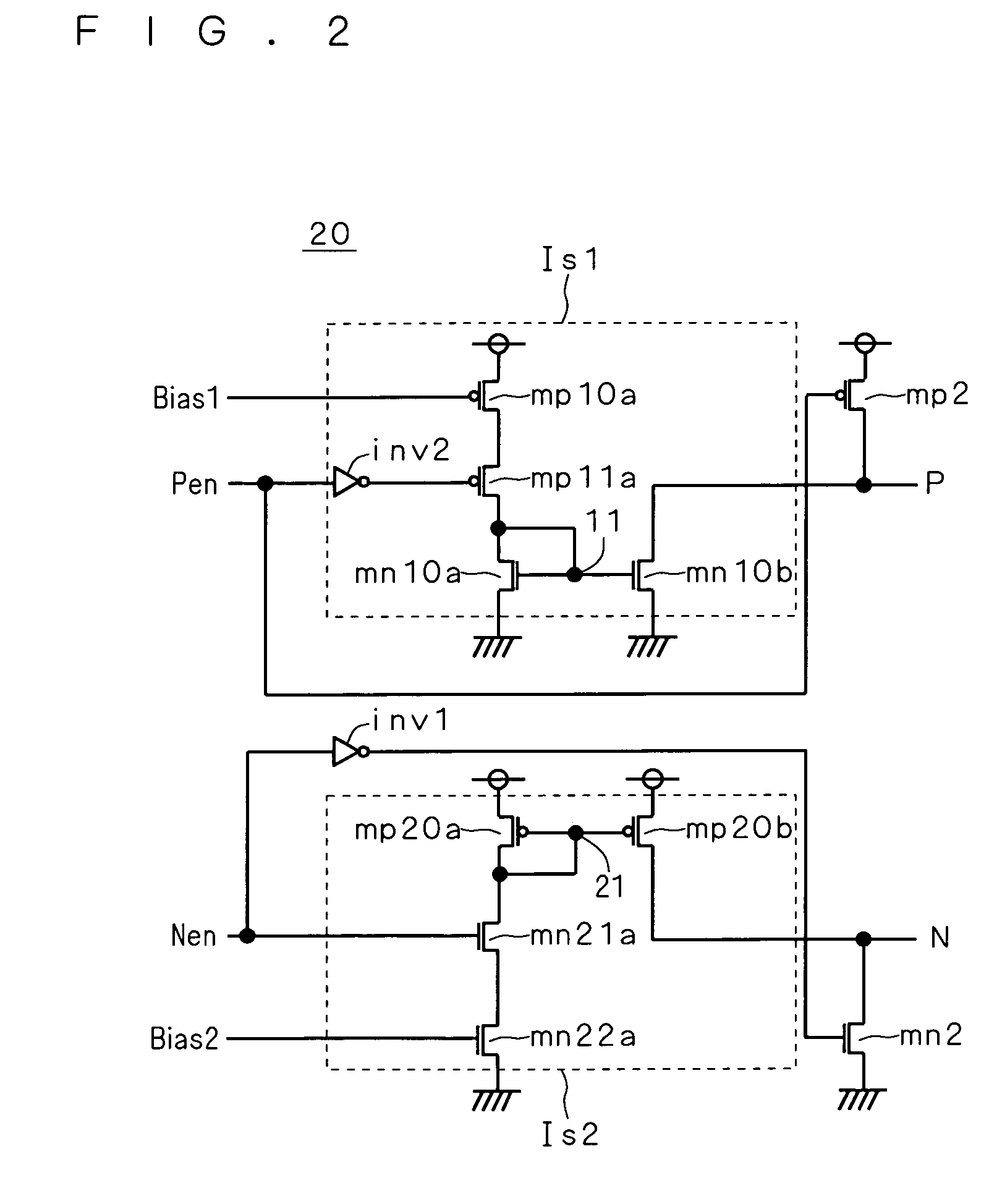
[0030]FIG. 1 shows a circuit diagram of the structure of a slew-rate controlled output buffer circuit 100 according to a first preferred embodiment. As shown, the output buffer circuit 100 includes a driver circuit 10, a driver control circuit 20 for controlling the driver circuit 10, and a capacitor circuit 30 interposed between the driver circuit 10 and the driver control circuit 20 for controlling a slew rate. FIG. 2 shows a circuit diagram of a detailed structure of the driver control circuit 20 shown in FIG. 1.

[0031]As shown in FIG. 1, the driver circuit 10 includes a PMOS transistor mp1 and an NMOS transistor mn1. The driver control circuit 20 includes constant current sources Is1 and Is2, a PMOS transistor mp2, an NMOS transistor mn2, and an inverter inv1. The capacitor circuit 30 includes capacitors C1 and C2, inverters inv3 and inv4, PMOS transistors mp4 and mp5, and NMOS transistors mn4 and mn5.

[0032]As shown in FIG. 2, the constant current source Is1 includes PMOS transis...

second preferred embodiment

[0069]In the output buffer circuit 100 shown in FIG. 1 according to the first preferred embodiment, the capacitors C1 and C2 are not connected to the node P or the node N at all times. It is therefore required that the node N be fixed to an H level (namely, the node A be fixed to an H level) when the signal Pen is switched from an L level to an H level and the signal Nen from an H level to an L level, for example. Accordingly, when the signals Pen and Nen have high frequencies, the potential of the node N cannot follow the switching of the signals Pen and Nen before being fixed to an H level, which may result in a variation in delay value.

[0070]FIG. 6 shows a circuit diagram of the structure of a slew-rate controlled output buffer circuit 100a according to a second preferred embodiment. FIG. 6 includes a capacitor circuit 30a instead of the capacitor circuit 30 shown in FIG. 1. The capacitor circuit 30a includes capacitors CP1, CP2, CN1, CN2, and an inverter inv5.

[0071]In the capaci...

third preferred embodiment

[0084]In the output buffer circuit 100a shown in FIG. 6 according to the second preferred embodiment, the capacitors CP2 and CN2 are out of contact with the node OUT, and are thus not used for slew rate control. Alternatively, the capacitors CP2 and CN2 may be disposed to come into contact with the node OUT, to be used for slew rate control.

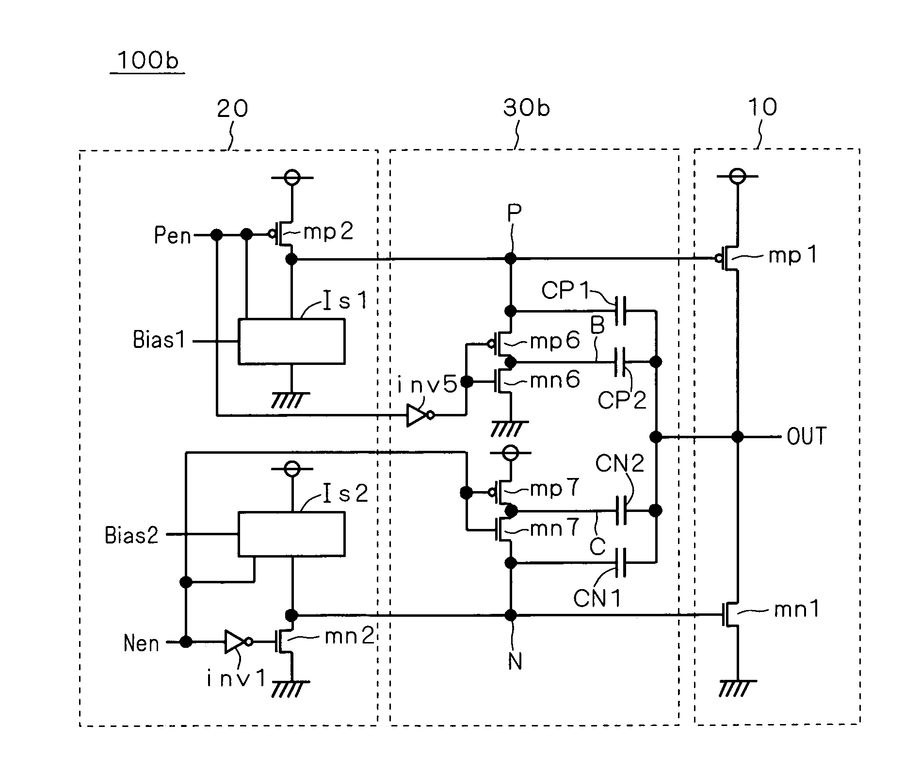
[0085]FIG. 7 shows a circuit diagram of the structure of a slew-rate controlled output buffer circuit 100b according to a third preferred embodiment. FIG. 7 includes a capacitor circuit 30b instead of the capacitor circuit 30 shown in FIG. 1. The capacitor circuit 30b includes the capacitors CP1, CP2, CN1, CN2, the inverter inv5, PMOS transistors mp6 and mp7, and NMOS transistors mn6 and mn7.

[0086]In the capacitor circuit 30b, the respective one ends of the capacitors CP1, CP2, CN1, and CN2 are connected to each other at the node OUT. The other end of the capacitor CP1 is connected at the node P to the gate of the PMOS transistor mp1, the drain o...


PUM


Abstract

When a first signal is switched from an L level to an H level and a second signal is switched from an H level to an L level, and a first constant current source cannot follow the switching immediately thereafter and has not yet been switched, a first node remains at an H level, so an output node remains at an L level. In such state, a second node having been connected to a third node of an H level before the switching becomes connected to the first node of an H level by the switching. At the same time, the output part of an inverter is switched from an H level to an L level, causing the second node to be switched from an H level to an L level as well via a capacitor. At this time, the potential of the first node is reduced to become equal to the second node, to make a transition to an L level.

Description

BACKGROUND OF THE INVENTION[0001]1. Field of the Invention[0002]The present invention relates to output buffer circuits and, more specifically, to techniques for reducing an output delay in slew-rate controlled output buffer circuits.[0003]2. Description of the Background Art[0004]Conventionally, an output buffer circuit includes a driver circuit that outputs a driver signal from an output node between a PMOS transistor for output and an NMOS transistor for output, a driver control circuit that controls the gates of the PMOS transistor for output and the NMOS transistor for output based on a supplied control signal, and a capacitor circuit that is interposed between the driver circuit and the driver control circuit, and controls a slew rate by using a capacitor.[0005]The slew rate of an output buffer circuit is defined by such standards as ATA / ATAPI, and strobe signal and data having a period of 30 nanoseconds are defined by such protocols as UltraDMA-mode 6. For this reason, there ...

Claims


Application Information

Patent Timeline
Patent Type & Authority Patents(United States)
IPC IPC(8): H03K3/00
CPCH03K17/04206H03K17/165H03K17/6872H03K19/00361
Inventor KANZAKI, TERUAKI
Owner RENESAS ELECTRONICS CORP
Why Eureka
Try Eureka