

Semiconductor memory apparatus
a memory apparatus and semiconductor technology, applied in the field of semiconductor memory apparatus, can solve the problems of slow precharging, increase in load and limit the package size used in a plurality of product groups, and achieve the effect of reducing the precharging time of local input/output lines
- Summary
- Abstract
- Description
- Claims
- Application Information
AI Technical Summary
Benefits of technology
Problems solved by technology
Method used
Image

Examples
Embodiment Construction
[0029]Hereinafter, an exemplary embodiment of the present invention will be described in detail with reference to the accompanying drawings.
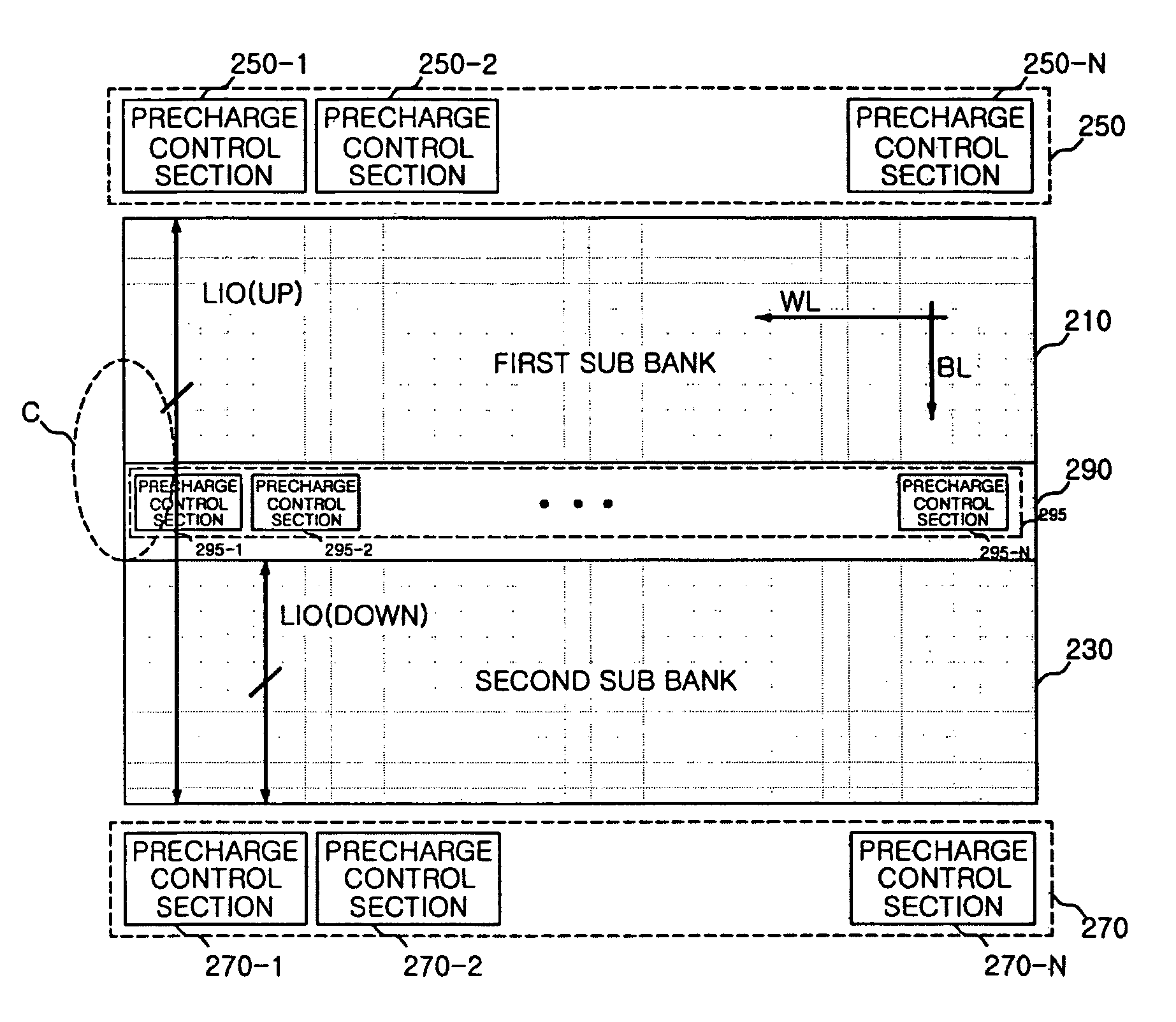
[0030]Referring to FIG. 3, a semiconductor memory apparatus according to an embodiment of the present invention includes a first sub bank 210, a second sub bank 230, a center bitline sense amplifier array 290, a first precharge section 250, a second precharge section 270, and a third precharge section 295.
[0031]The center bitline sense amplifier array 290 is arranged in a region where the first sub bank 210 meets the second sub bank 230. The first precharge section 250 is arranged above the first sub bank 210 and precharges local input / output lines LIO of the first sub bank 210 and the second sub bank 230. The second precharge section 270 is arranged below the second sub bank 230 and precharges the local input / output lines LIO. The third precharge section 295 is arranged in the center bitline sense amplifier array 290 and precharges the local in...
PUM
 Abstract
Description
Claims
Application Information