Methods of forming wiring to transistor and related transistor

a technology of wiring and transistors, applied in the direction of electrical equipment, semiconductor devices, semiconductor/solid-state device details, etc., can solve the problems of affecting the performance of fets

Inactive Publication Date: 2010-02-23
GLOBALFOUNDRIES INC
View PDF4 Cites 221 Cited by
  • Summary
  • Abstract
  • Description
  • Claims
  • Application Information

AI Technical Summary

Benefits of technology

[0010]The illustrative aspects of the present disclosure are designed to solve the problems herein described and / or other problems not discussed.

Problems solved by technology

In current field effect transistor (FET) technology, contacts between FETs and a first metal layer are becoming a significant problem for continued scaling.
Furthermore, each contact has a significant amount of parasitic capacitance between itself and the gate, which degrades the FET performance.
In addition, the contacts have high and potentially quite varied resistance due to their small size and high aspect ratio, which also degrades the FET performance.
The contacts also require holes in the stress / strain generating layers, relaxing some of the stress / strain and decreasing FET performance.
Overall, processing of these devices is much more complicated and new methods to simplify their fabrication are desirable.
The extra layer adds complexity, costs and size.

Method used


Image

  • Methods of forming wiring to transistor and related transistor
  • Methods of forming wiring to transistor and related transistor
  • Methods of forming wiring to transistor and related transistor

Examples


Embodiment Construction

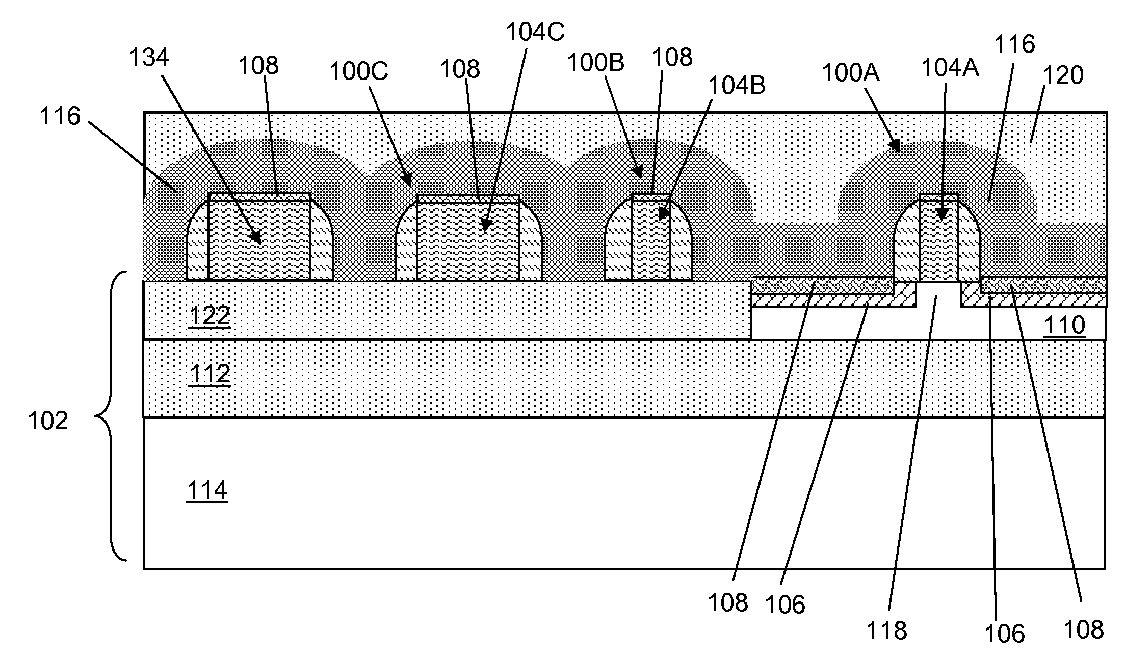
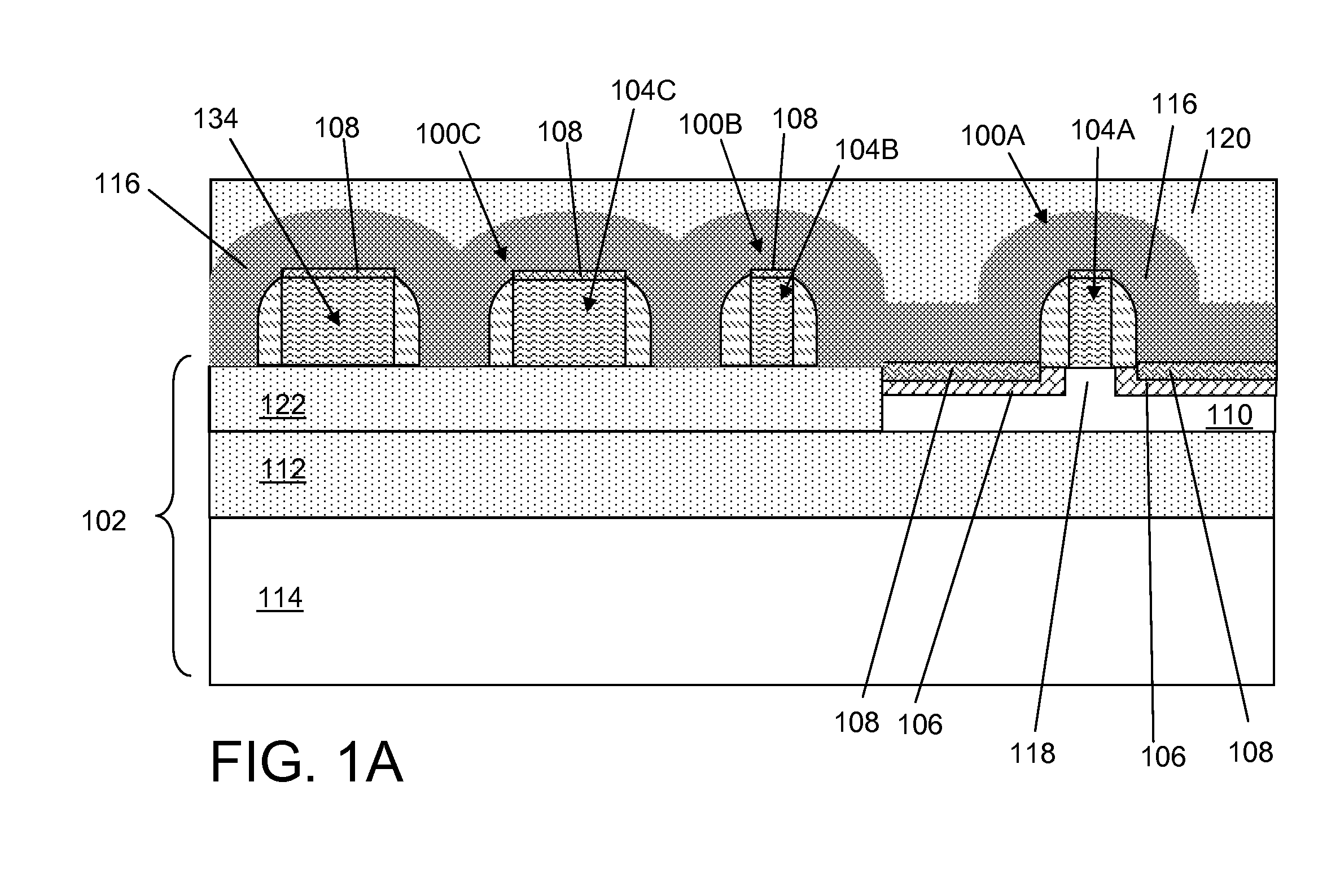
[0020]Turning to the drawings, FIGS. 1A-7 show embodiments of a method of forming wiring to a transistor, with FIG. 7 showing embodiments of a transistor 100A-C including the wiring. In one embodiment shown in FIG. 1A, a transistor 100A-C is formed on a semiconductor-on-insulator (SOI) substrate 102 using masks that are mirror images of an intended layout. Mirror image masks are required, as will become apparent below, because transistor 100A-C is ultimately flipped over. As illustrated, the forming includes forming a gate 104A-C (no gate dielectric shown), a source / drain region 106 and associated silicide 108 for each, and a channel 118. (Note, channel 118 is shown only for transistor 100A, but may be present for transistors 100B-C at another location, e.g., into or out of the plane of the page.) As shown in FIG. 1A, transistor 100A-C forming may also include forming an isolation region 122 for transistor 100A-C. Isolation region 122 is formed between transistors to provide isolati...


PUM


Abstract

Methods of wiring to a transistor and a related transistor are disclosed. In one embodiment, the method includes a method of forming wiring to a transistor, the method comprising: forming a transistor on a semiconductor-on-insulator (SOI) substrate using masks that are mirror images of an intended layout, the forming including forming a gate and a source / drain region for each and a channel, the SOI substrate including a semiconductor-on-insulator (SOI) layer, a buried insulator layer and a silicon substrate; forming a dielectric layer over the transistor; bonding the dielectric layer to another substrate; removing the silicon substrate from the SOI substrate to the buried insulator layer; forming a contact to each of the source / drain region and the gate from a channel side of the gate; and forming at least one wiring to the contacts on the channel side of the gate.

Description

BACKGROUND[0001]1. Technical Field[0002]The disclosure relates generally to integrated circuit (IC) chip fabrication, and more particularly, to methods of forming wiring to a transistor and a related transistor.[0003]2. Background Art[0004]In current field effect transistor (FET) technology, contacts between FETs and a first metal layer are becoming a significant problem for continued scaling. In particular, in order for contacts to reach source / drain regions between the gates of adjacent FETs, they must be extremely tall. Consequently, they must be fabricated with extremely steep sidewalls, very high aspect ratios, very tiny cross sectional area, and very tight alignment tolerances in order to squeeze them into the small space available between the gates. Furthermore, each contact has a significant amount of parasitic capacitance between itself and the gate, which degrades the FET performance. In addition, the contacts have high and potentially quite varied resistance due to their ...

Claims


Application Information

Patent Timeline
Patent Type & Authority Patents(United States)
IPC IPC(8): H01L21/84
CPCH01L21/768H01L21/76898H01L23/481H01L29/78H01L29/66477H01L2924/0002H01L2924/00
Inventor FRANK, DAVID J.LA TULIPE, JR., DOUGLAS C.STEEN, STEVEN E.TOPOL, ANNA W.
Owner GLOBALFOUNDRIES INC
Why Eureka
Try Eureka