Semiconductor transistors having high-K gate dielectric layers, metal gate electrode regions, and low fringing capacitances

a technology of semiconductor transistors and dielectric layers, which is applied in the direction of semiconductor devices, electrical equipment, transistors, etc., can solve the problems of affecting the operation of transistors by fringing capacitances between the gate electrode region and the source/drain region of the transistor,

Inactive Publication Date: 2010-02-23
GLOBALFOUNDRIES INC
View PDF16 Cites 9 Cited by
  • Summary
  • Abstract
  • Description
  • Claims
  • Application Information

AI Technical Summary

Problems solved by technology

In a typical transistor with a high-K gate dielectric layer and a metal gate electrode region, the fringing capacitances between the gate electrode region and the source / drain regions of the transistor detrimentally affect the operation of the transistor.

Method used


Image

  • Semiconductor transistors having high-K gate dielectric layers, metal gate electrode regions, and low fringing capacitances
  • Semiconductor transistors having high-K gate dielectric layers, metal gate electrode regions, and low fringing capacitances
  • Semiconductor transistors having high-K gate dielectric layers, metal gate electrode regions, and low fringing capacitances

Examples


Embodiment Construction

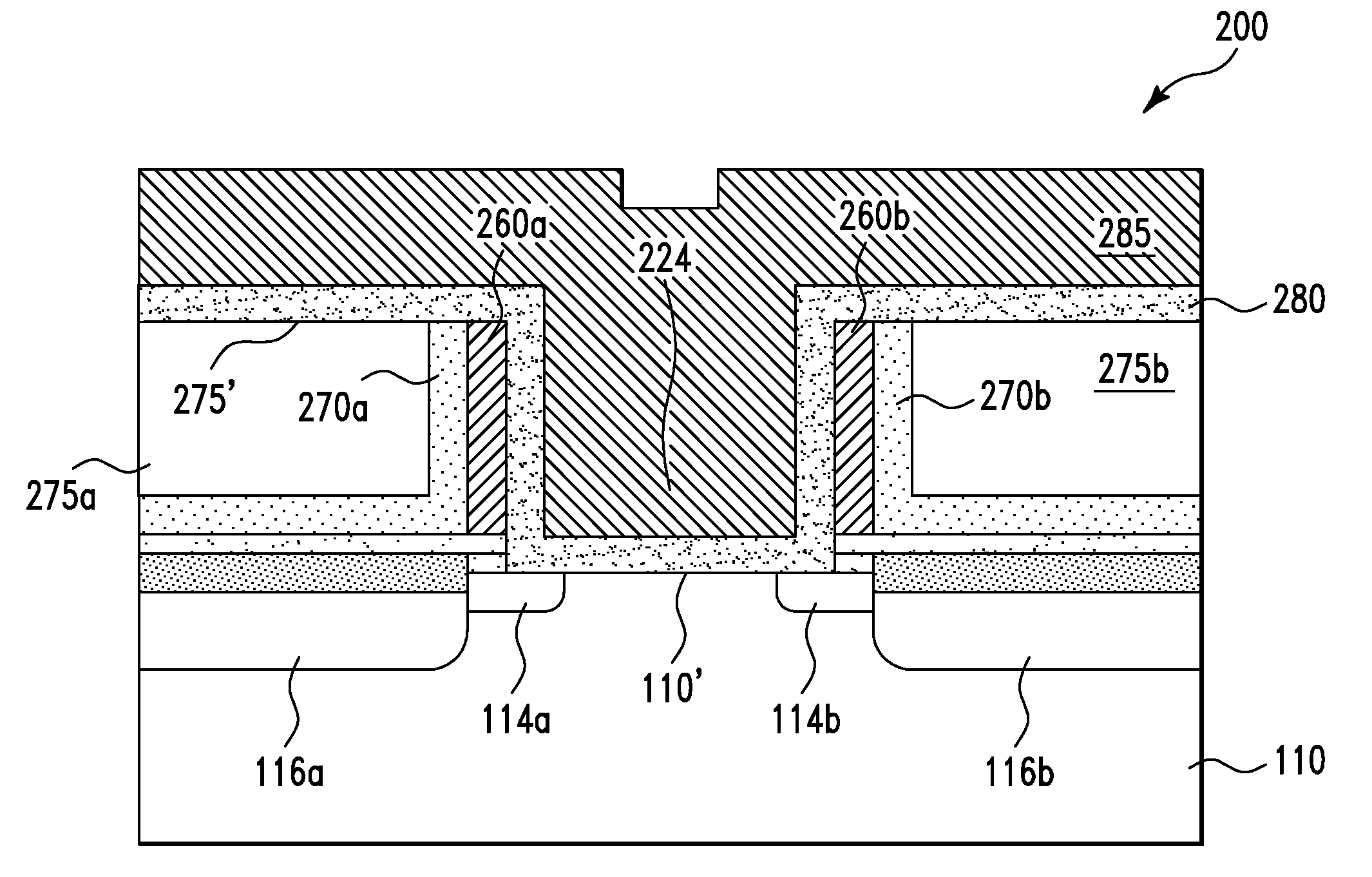
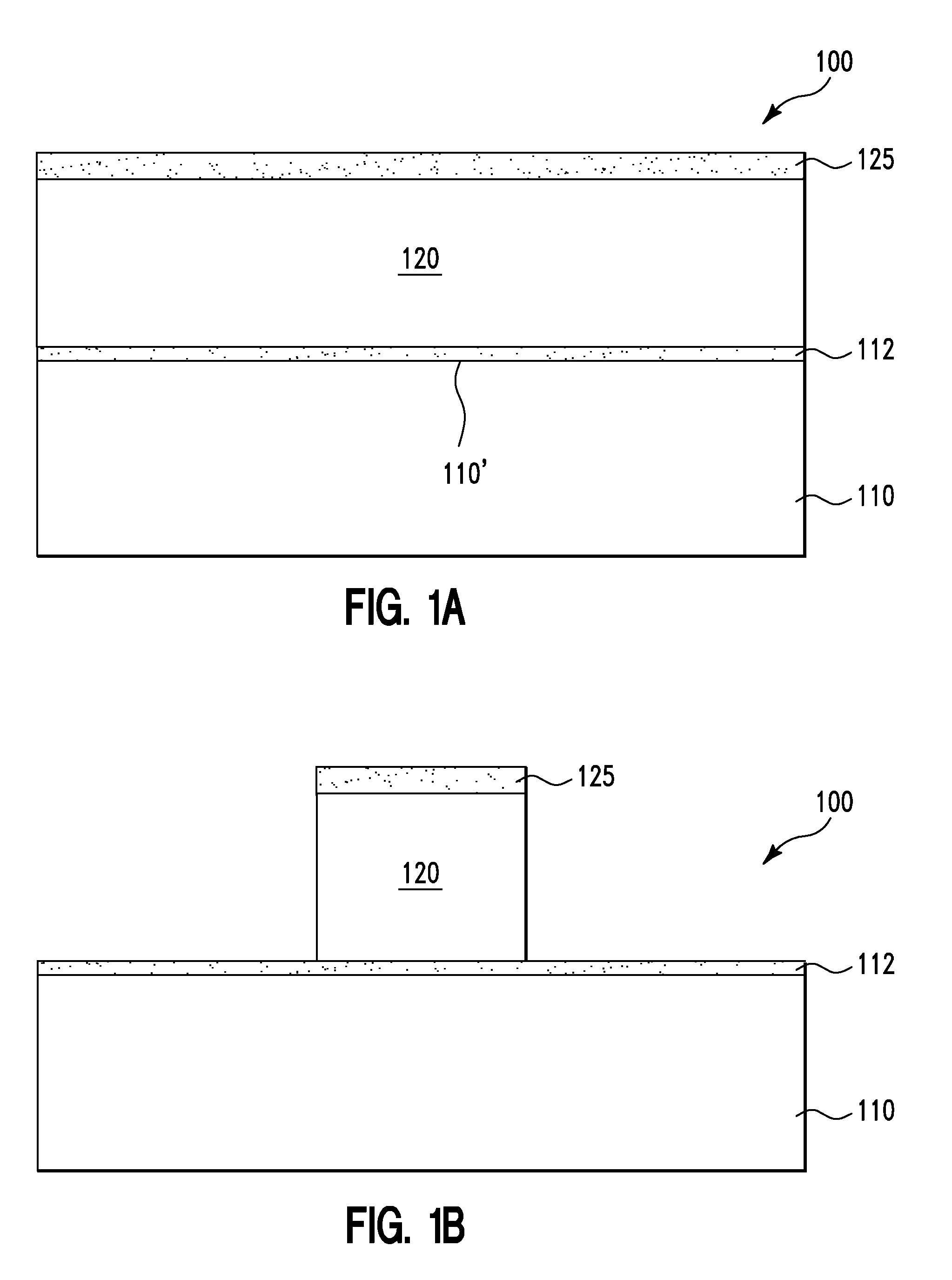
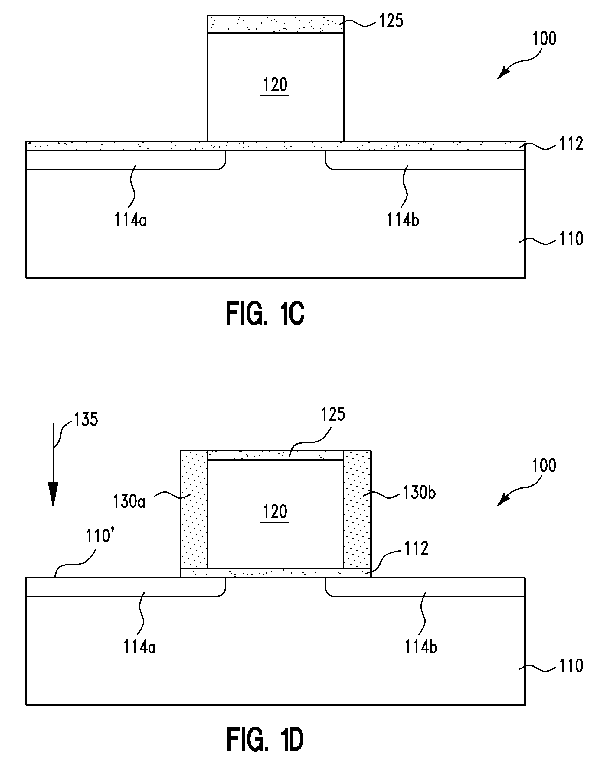
[0007]FIGS. 1A-1Q show cross-section views used to illustrate a fabrication process of a semiconductor structure 100, in accordance with embodiments of the present invention. More specifically, with reference to FIG. 1A, the fabrication process of the semiconductor structure 100 can start with a silicon substrate 110.

[0008]Next, in one embodiment, a temporary gate dielectric layer 112 is formed on top of the silicon substrate 110. The temporary gate dielectric layer 112 can comprise silicon dioxide. The temporary gate dielectric layer 112 can be formed by thermally oxidizing the top surface 110′ of the silicon substrate 110 resulting in the temporary gate dielectric layer 112.

[0009]Next, in one embodiment, a temporary gate electrode layer 120 is formed on top of the temporary gate dielectric layer 112. The temporary gate electrode layer 120 can comprise poly-silicon. The temporary gate electrode layer 120 can be formed by CVD (Chemical Vapor Deposition) of poly-silicon on top of the...


PUM


Abstract

A semiconductor structure and a method for forming the same. The structure includes (i) a semiconductor substrate which includes a channel region, (ii) first and second source / drain regions on the semiconductor substrate, (iii) a gate dielectric region, and (iv) a gate electrode region, (v) a plurality of interconnect layers on the gate electrode region, and (vi) first and second spaces. The gate dielectric region is disposed between and in direct physical contact with the channel region and the gate electrode region. The gate electrode region is disposed between and in direct physical contact with the gate dielectric region and the interconnect layers. The first and second spaces are in direct physical contact with the gate electrode region. The first space is disposed between the first source / drain region and the gate electrode region. The second space is disposed between the second source / drain region and the gate electrode region.

Description

FIELD OF THE INVENTION[0001]The present invention relates generally to semiconductor transistors and more particularly to semiconductor transistors having high-K gate dielectric layers, metal gate electrode regions, and low fringing capacitances.BACKGROUND OF THE INVENTION[0002]In a typical transistor with a high-K gate dielectric layer and a metal gate electrode region, the fringing capacitances between the gate electrode region and the source / drain regions of the transistor detrimentally affect the operation of the transistor. Therefore, there is a need for a structure (and a method for forming the same) in which the fringing capacitances are lower than those of the prior art.SUMMARY OF THE INVENTION[0003]The present invention provides a semiconductor structure fabrication method, comprising providing a semiconductor structure which includes (i) a semiconductor substrate which includes a channel region, (ii) a first source / drain region on the semiconductor substrate, (iii) a secon...

Claims


Application Information

Patent Timeline
Patent Type & Authority Patents(United States)
IPC IPC(8): H01L21/00
CPCH01L29/4983H01L29/6653H01L29/66545H01L29/6659H01L29/7833H01L29/4966H01L29/518Y10S257/90
Inventor GAMBINO, JEFFREY PETER
Owner GLOBALFOUNDRIES INC
Why Eureka
Try Eureka