Pixel having two semiconductor layers, image sensor including the pixel, and image processing system including the image sensor

a technology of image sensor and semiconductor layer, applied in the field of image sensor pixels, can solve the problems of increasing production cost, limiting the “megapixel” capacity and color sensitivity of image sensor, and limiting the image quality of images captured by digital cameras

Active Publication Date: 2010-03-02
SAMSUNG ELECTRONICS CO LTD
View PDF10 Cites 56 Cited by
  • Summary
  • Abstract
  • Description
  • Claims
  • Application Information

AI Technical Summary

Problems solved by technology

The “MegaPixel” capacity and color sensitivity of image sensors is currently a limiting factor limiting image quality of images captured by digital cameras.
Thus, there is a limitation of the conventional image sensor due to a fill factor that represents the area occupied in a pixel by the photodiode.
To overcome this limitation, some have proposed an array of microlenses to be placed on top of the sensors, but this increases the production cost.
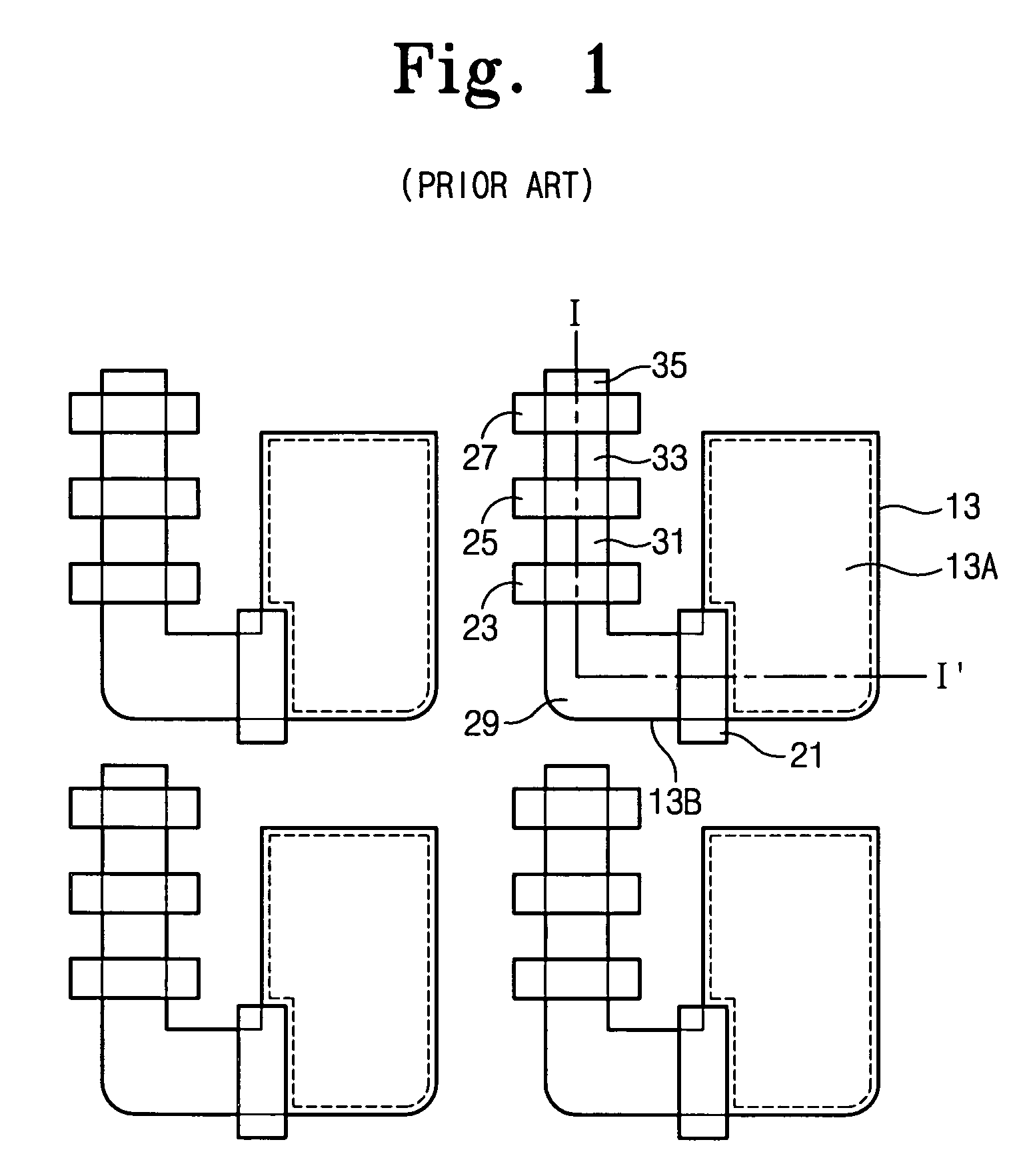
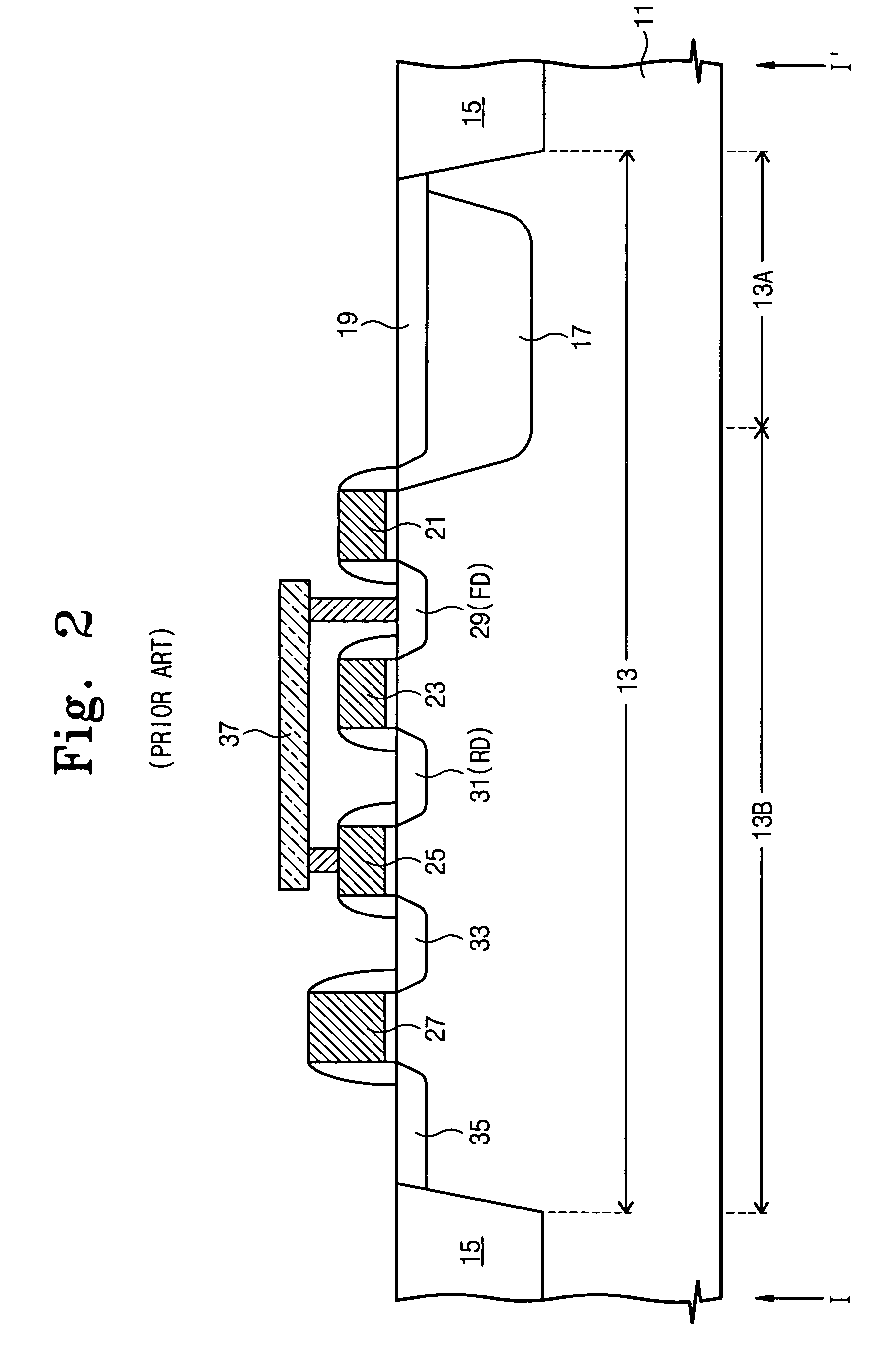
Additionally, in the conventional image sensor, light incident upon a target pixel, especially, light incident from a slanted angle, may be reflected by an interconnection of the target pixel or a gate and may arrive at an adjacent pixel, causing across-talk affect or distortion.

Method used


Image

  • Pixel having two semiconductor layers, image sensor including the pixel, and image processing system including the image sensor
  • Pixel having two semiconductor layers, image sensor including the pixel, and image processing system including the image sensor
  • Pixel having two semiconductor layers, image sensor including the pixel, and image processing system including the image sensor

Examples


Embodiment Construction

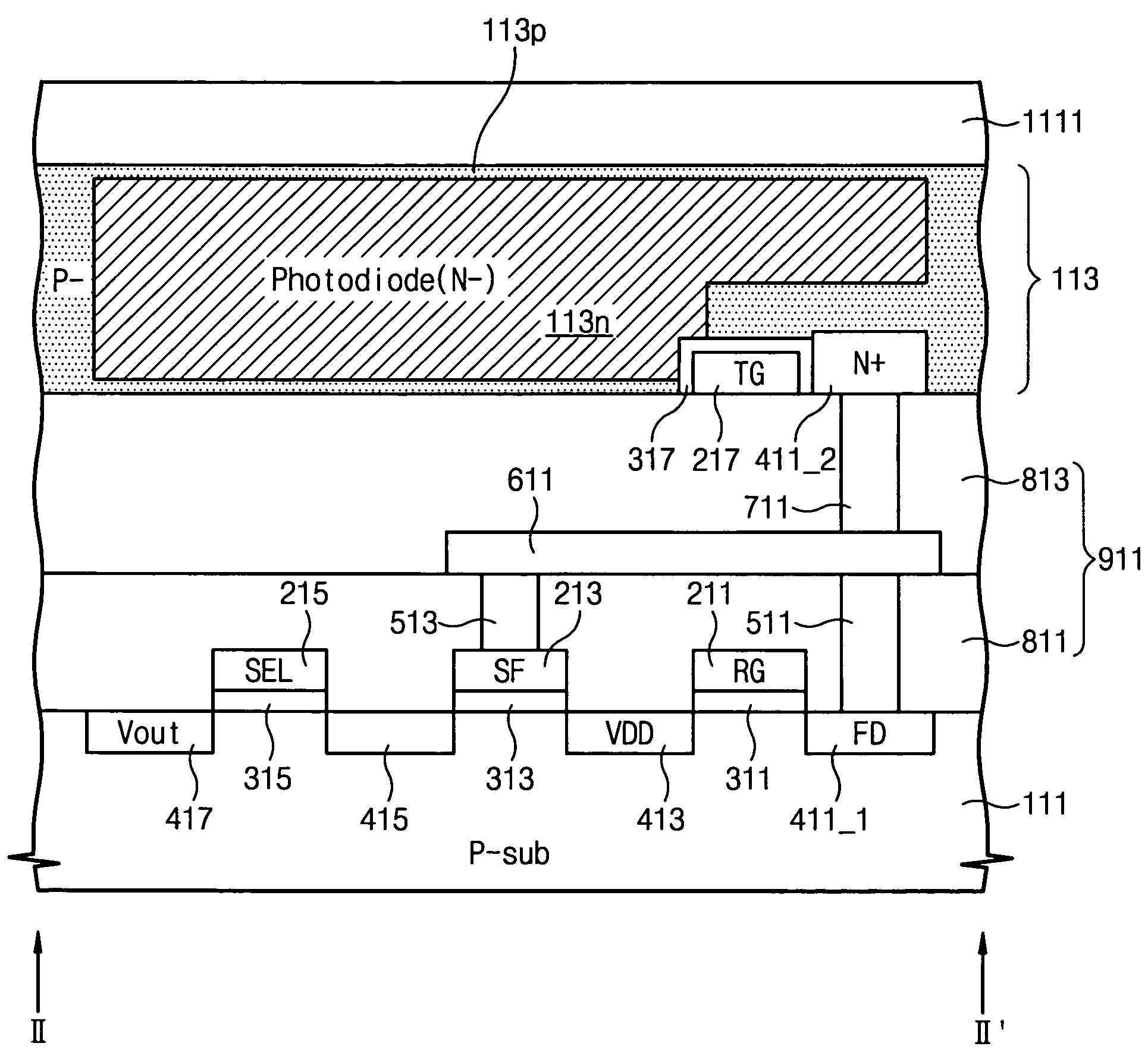
[0042]FIG. 3 is a perspective view of a pixel in an image sensor in accordance with an embodiment of the invention. Referring to FIG. 3, a pixel 101 according to the embodiment by the invention comprises a photodiode 115, and transfer, reset, source follower, and selection transistors operationally coupled with the photodiode 115. According to this embodiment of the invention, the components of the pixel 101 are arranged in separate first and second semiconductor patterns 111 and 113 that are spaced apart from each other. In this exemplary embodiment of the invention, the photodiode 115 and the transfer transistor are disposed in the second semiconductor pattern 113, while the reset, source follower, and selection transistors are placed in the first semiconductor pattern 111. The gate 217 of the transfer transistor is disposed under the photodiode 115. Thus, the fill factor of the pixel is not affected by the presence or size of the transfer, reset, source follower, and selection tr...


PUM


Abstract

An image sensor having pixels that include two patterned semiconductor layers. The top patterned semiconductor layer contains the photoelectric elements of pixels having substantially 100% fill-factor. The bottom patterned semiconductor layer contains transistors for detecting, resetting, amplifying and transmitting signals charges received from the photoelectric elements. The top and bottom patterned semiconductor layers may be separated from each other by an interlayer insulating layer that may include metal interconnections for conducting signals between devices formed in the patterned semiconductor layers and from external devices.

Description

CROSS-REFERENCE TO RELATED APPLICATIONS[0001]This U.S. non-provisional patent application claims priority under 35 U.S.C. §119 of Korean Patent Application 2005-91293 filed on Sep. 29, 2005, the entire contents of which are hereby incorporated by reference.BACKGROUND[0002]The present invention relates to image sensors, and more particularly to pixels of image sensors.[0003]Digital cameras are today one of the most popular consumer electronics. The “MegaPixel” capacity and color sensitivity of image sensors is currently a limiting factor limiting image quality of images captured by digital cameras. Image sensors function to transform (visible) light that is focused onto the image sensor by optical lenses, into electrical signals to capture and display images of high quality. Additionally, a very fast “shutter speed” or “film speed” equivalent in digital image sensors is a strong selling point for high-end digital cameras and can enhance image quality (e.g., reducing blurring due to s...

Claims


Application Information

Patent Timeline
Patent Type & Authority Patents(United States)
IPC IPC(8): H01L31/062
CPCH01L27/14634H01L27/1464H01L27/14643H01L27/14612H01L27/14636H01L27/146
Inventor AHN, JUNG-CHAK
Owner SAMSUNG ELECTRONICS CO LTD
Why Eureka
Try Eureka