Multiple-core processor with flexible mapping of processor cores to cache banks

a multi-core processor and cache bank technology, applied in the field of processors, can solve the problems of high transistor count manufacturing devices, high cost per unit, and low yield of high-quality scrapped parts

Active Publication Date: 2010-03-23
ORACLE INT CORP
View PDF48 Cites 89 Cited by
  • Summary
  • Abstract
  • Description
  • Claims
  • Application Information

AI Technical Summary

Problems solved by technology

Despite advances in integrated circuit fabrication processes, manufacturing devices having high transistor counts can be difficult.
The number of transistors on an integrated circuit device results is correlated to the number of opportunities for defects to occur during the manufacturing process.
The large number of defect opportunities present in the manufacturing process may in turn lead to a low yield and a significant number of scrapped parts.
The low manufacturing yield may result in a higher per-unit cost for good units, and in some cases can make the manufacture of a design economically unfeasible.
However, given the complexity and expense of designing a single version of a processor or other integrated circuit having a large transistor count, it may be impractical to separately design and manufacture a processor for each of several different market segments.

Method used


Image

  • Multiple-core processor with flexible mapping of processor cores to cache banks
  • Multiple-core processor with flexible mapping of processor cores to cache banks
  • Multiple-core processor with flexible mapping of processor cores to cache banks

Examples


Embodiment Construction

Overview of Multithreaded Processor Architecture

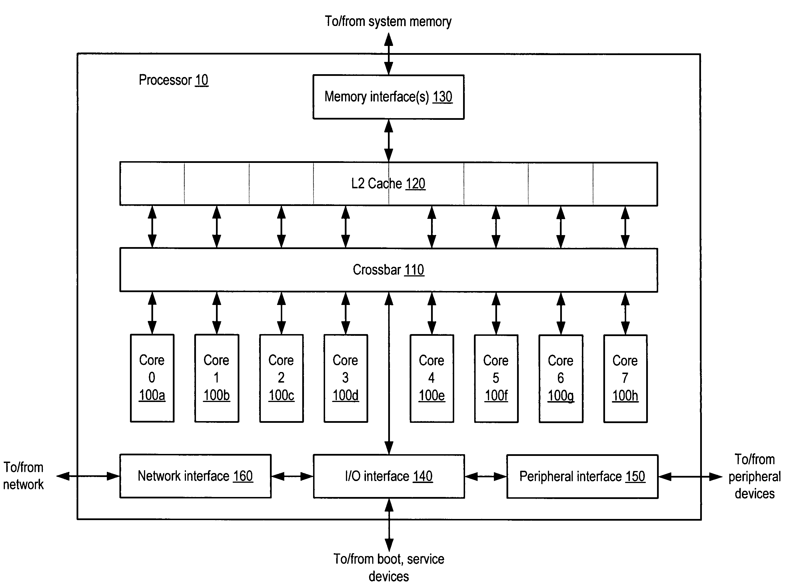
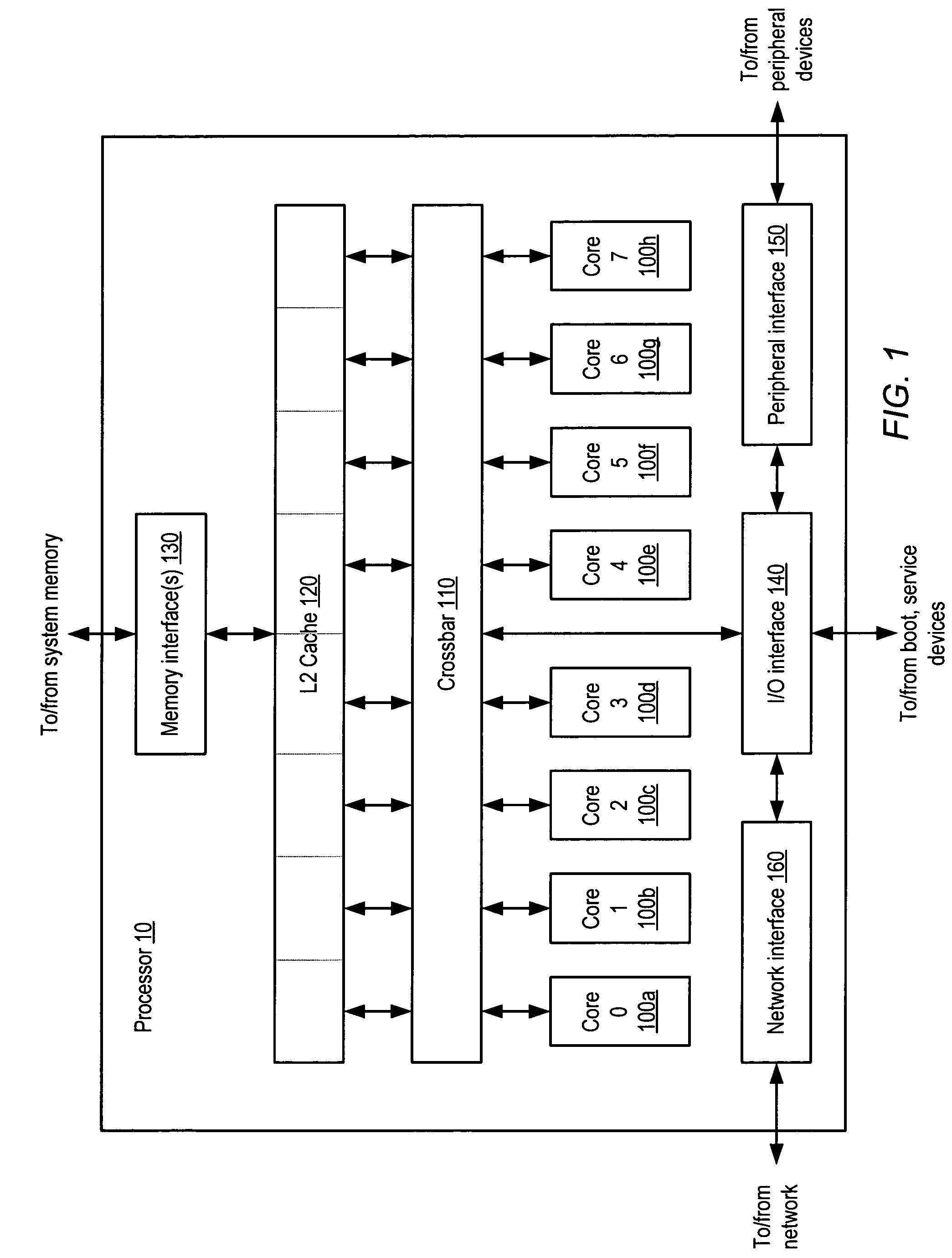
[0031]A block diagram-illustrating one embodiment of a multithreaded processor 10 is shown in FIG. 1. In the illustrated embodiment, processor 10 includes a plurality of processor cores 100a-h, which are also designated “core 0” though “core 7”. Each of cores 100 is coupled to an L2 cache 120 via a crossbar 110. L2 cache 120 is coupled to one or more memory interface(s) 130, which are coupled in turn to one or more banks of system memory (not shown). Additionally, crossbar 110 couples cores 100 to input / output (I / O) interface 140, which is in turn coupled to a peripheral interface 150 and a network interface 160. As described in greater detail below, I / O interface 140, peripheral interface 150 and network interface 160 may respectively couple processor 10 to boot and / or service devices, peripheral devices, and a network.

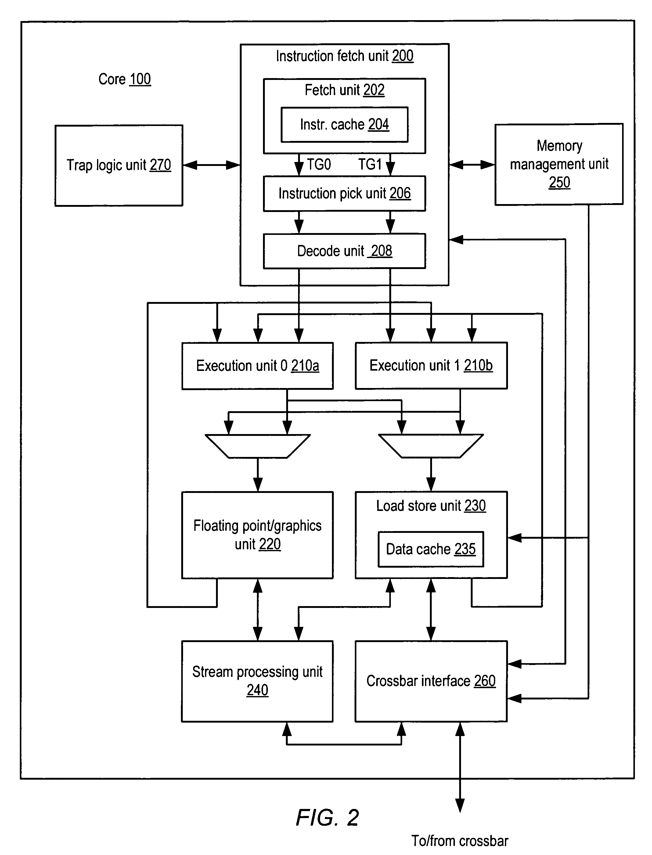
[0032]Cores 100 may be configured to execute instructions and to process data according to a particular instruction s...


PUM


Abstract

A multiple-core processor providing flexible mapping of processor cores to cache banks. In one embodiment, a processor may include a cache including a number of cache banks. The processor may further include a number of processor cores configured to access the cache banks, as well as core/bank mapping logic coupled to the cache banks and processor cores. The core/bank mapping logic may be configurable to map a cache bank select portion of a memory address specified by a given one of the processor cores to any one of the cache banks.

Description

PRIORITY CLAIM[0001]This application claims benefit of priority of U.S. Provisional Patent Application No. 60 / 584,064, entitled“Yield Recovery Technique for Integrated Circuits” and filed on Jun. 30, 2004.BACKGROUND OF THE INVENTION[0002]1. Field of the Invention[0003]This invention relates to processors, and more particularly, to techniques for mapping memory accesses from processor cores to cache banks within a processor.[0004]2. Description of the Related Art[0005]With increasing demands on functionality and performance as well as improved fabrication techniques, newer generations of processors and other integrated circuits have significantly higher levels of integration than their predecessors. Transistor counts in the hundreds of millions on an integrated circuit are not uncommon, and transistor counts of over one billion are inevitable.[0006]Despite advances in integrated circuit fabrication processes, manufacturing devices having high transistor counts can be difficult. The n...

Claims


Application Information

Patent Timeline
Patent Type & Authority Patents(United States)
IPC IPC(8): G06F12/00G06F12/06
CPCG06F12/084G06F12/0846G06F2212/601
Inventor HETHERINGTON, RICKY C.SHAH, MANISH K.GROHOSKI, GREGORY F.SAHA, BIKRAM
Owner ORACLE INT CORP
Why Eureka
Try Eureka