EEPROM array with well contacts

a well contact and array technology, applied in the direction of digital storage, instruments, transistors, etc., can solve the problem that the repetition arrangement cannot be maintained in the portions of cell well bias lines and cell well contacts

Active Publication Date: 2010-04-06
KIOXIA CORP
View PDF8 Cites 5 Cited by
  • Summary
  • Abstract
  • Description
  • Claims
  • Application Information

AI Technical Summary

Problems solved by technology

However, the repetitive arrangement cannot be maintained in the portions of the cell well bias lines and cell well contacts.

Method used


Image

  • EEPROM array with well contacts
  • EEPROM array with well contacts
  • EEPROM array with well contacts

Examples


Embodiment Construction

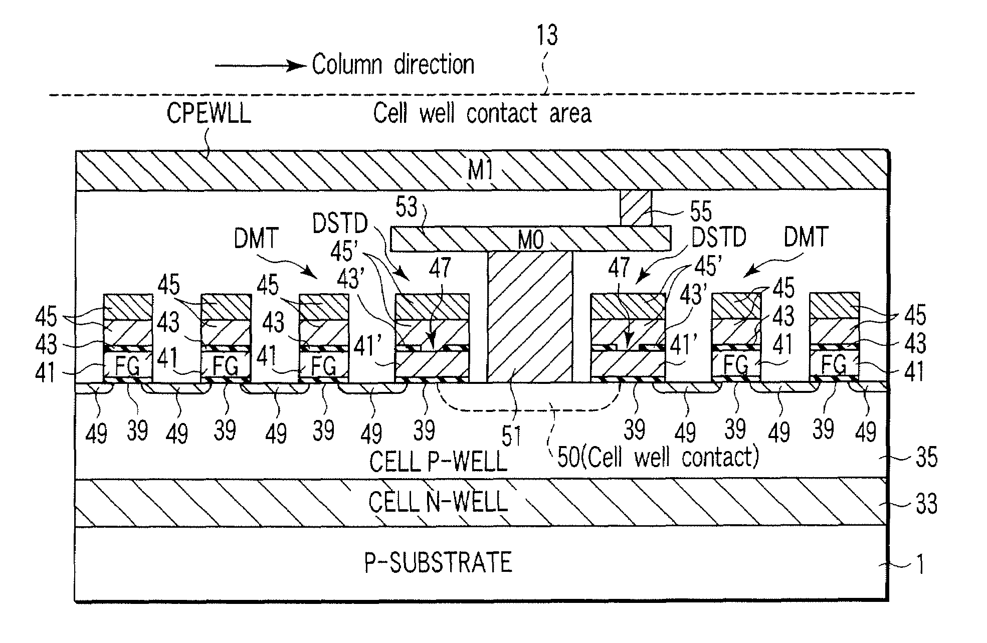
[0030]One of the important factors when a semiconductor integrated circuit device is miniaturized is the lithography technology. It becomes possible to transfer a fine pattern onto the semiconductor integrated circuit device by enhancing the resolution of the lithography technology. In order to enhance the resolution, it is important to pay much attention to the lithography technology itself, for example, the condition of illumination and formation of a photomask.

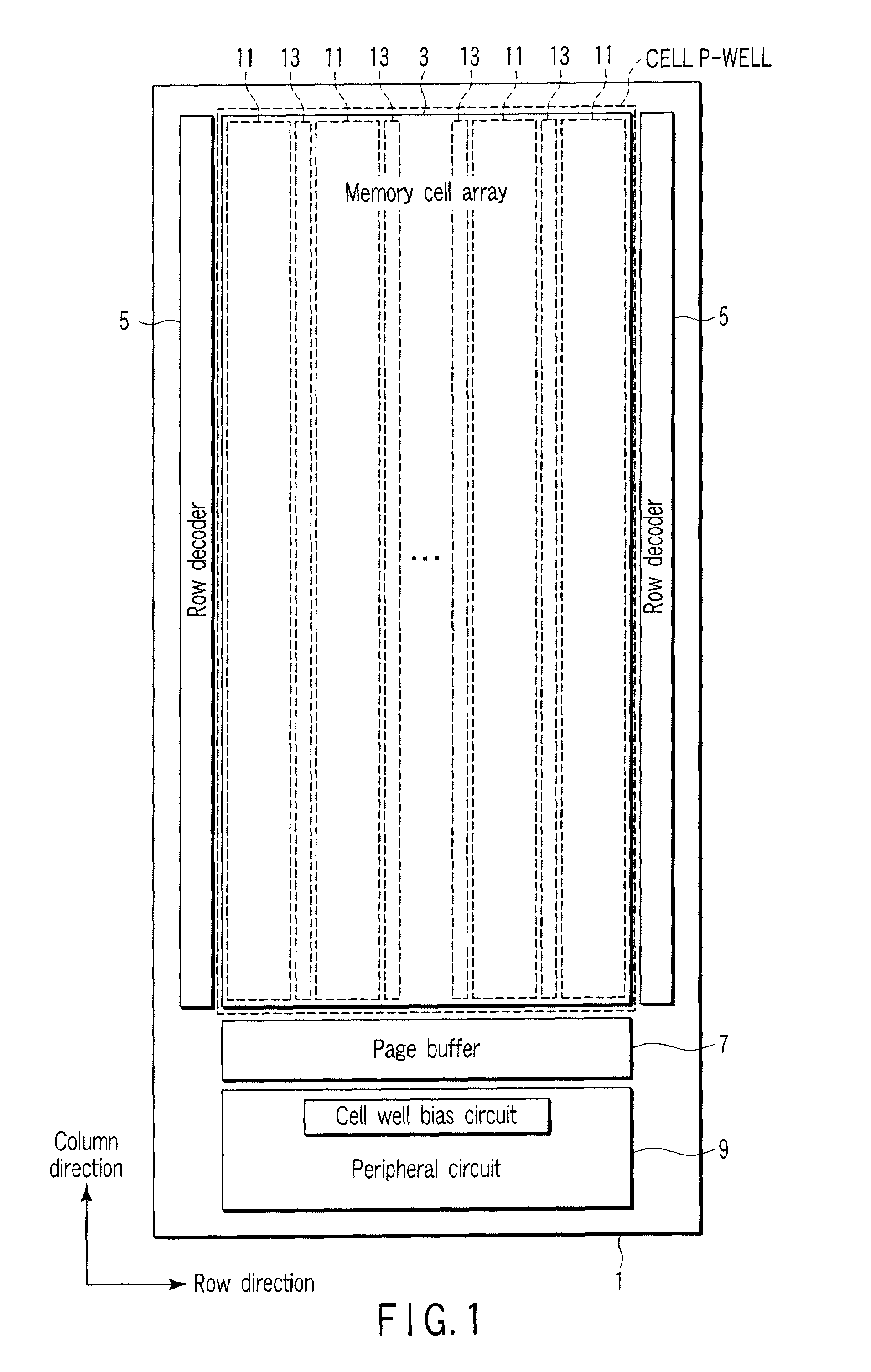
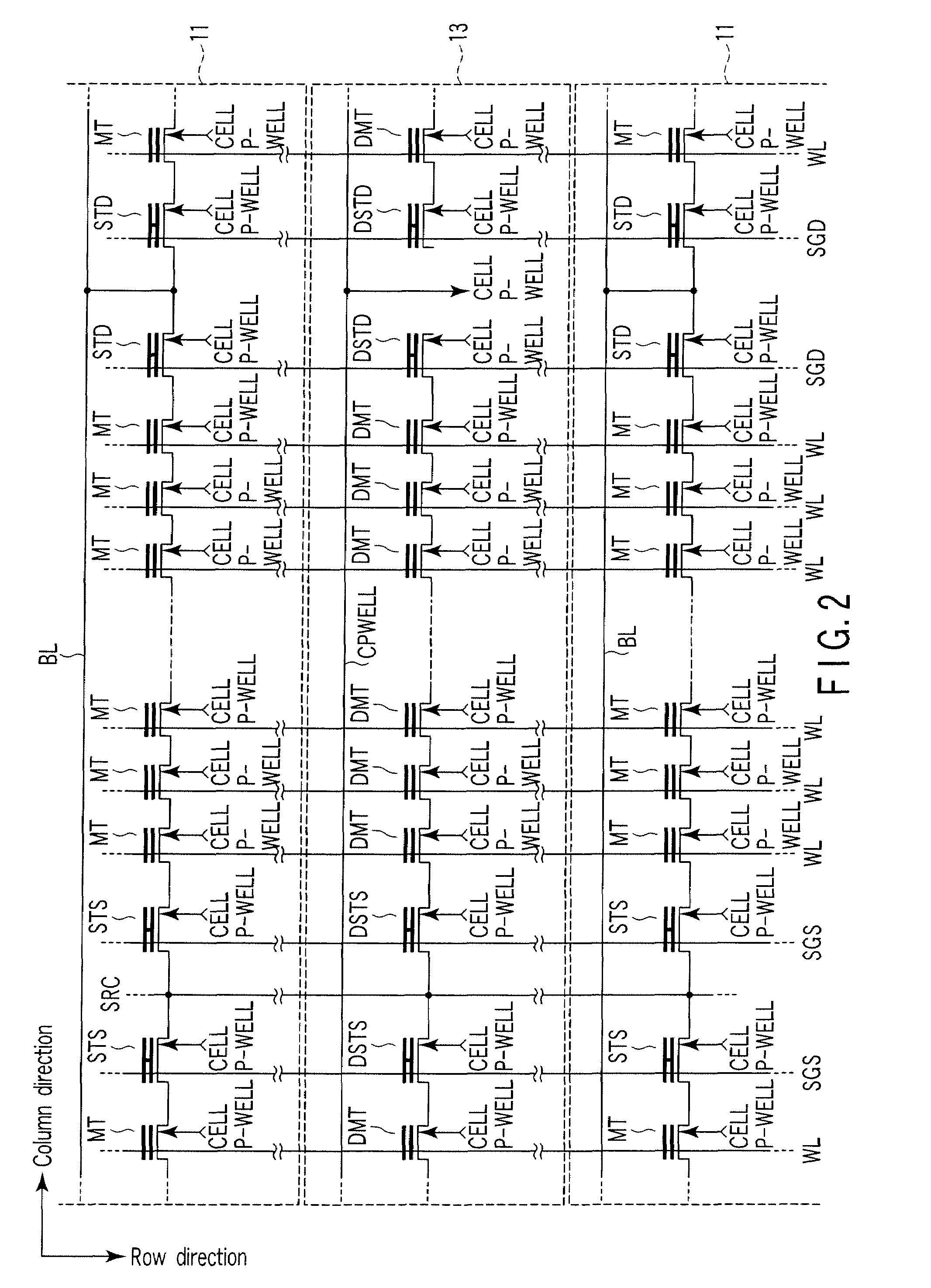
[0031]Further, it is also important to pay much attention to the semiconductor integrated circuit device itself by providing a layout pattern which can be easily resolved. For example, if the repetitive arrangement of bit lines and word lines is lost and the repetitive arrangement of block selection lines, cell source lines and floating gate layers is lost when they are used, a problem which obstructs the development of the fine patterning technique may occur. The present embodiment relates to the technique for improving th...


PUM


Abstract

A semiconductor integrated circuit device includes a cell well, a memory cell array formed on the cell well and having a memory cell area and cell well contact area, first wiring bodies arranged in the memory cell area, and second wiring bodies arranged in the cell well contact area. The layout pattern of the second wiring bodies is the same as the layout pattern of the first wiring bodies. The cell well contact area comprises cell well contacts that have the same dopant type as the cell well and that function as source / drain regions of dummy transistors formed in the cell well contact area.

Description

CROSS REFERENCE TO RELATED APPLICATIONS[0001]This is a Continuation Application of PCT Application No. PCT / JP2005 / 017206, filed Sep. 12, 2005, which was published under PCT Article 21(2) in English.[0002]This application is based upon and claims the benefit of priority from prior Japanese Patent Application No. 2005-100955, filed Mar. 31, 2005, the entire contents of which are incorporated herein by reference.BACKGROUND OF THE INVENTION[0003]1. Field of the Invention[0004]This invention relates to a semiconductor integrated circuit device and more particularly to a semiconductor integrated circuit device having a nonvolatile semiconductor memory.[0005]2. Description of the Related Art[0006]EEPROMs are known as semiconductor memories, for example, nonvolatile semiconductor memories. Some EEPROMs have wells whose potential can be changed and memory cell transistors formed on the wells. As a representative example thereof, a flash memory, for example, a NAND flash memory in which data ...

Claims


Application Information

Patent Timeline
Patent Type & Authority Patents(United States)
IPC IPC(8): H01L29/24G11C16/04
CPCH01L27/0207H01L27/115H01L27/11521H01L27/11524H01L27/11519H01L27/105H01L27/11529H10B41/10H10B41/41H10B41/35H10B69/00H10B41/30H01L27/04H10B99/00
Inventor SATO, ATSUHIROSUGIMAE, KIKUKOICHIGE, MASAYUKI
Owner KIOXIA CORP
Why Eureka
Try Eureka