Method and apparatus for angular high density plasma chemical vapor deposition

a high-density plasma and chemical vapor deposition technology, applied in the field of high-density plasma chemical vapor deposition (hdp) apparatus, can solve the problems of time-consuming, adversely affecting the overall product yield, and adding cost and complexity to the manufacturing process

Inactive Publication Date: 2012-07-26
ALSEPHINA INNOVATIONS INC
View PDF7 Cites 5 Cited by
  • Summary
  • Abstract
  • Description
  • Claims
  • Application Information

AI Technical Summary

Problems solved by technology

Each process step adds cost and complexity to the manufacturing process, and may adversely affect overall product yield.
This technique is time-consuming, and the multiple masking and etching steps add to the manufacturing costs accordingly.

Method used


Image

  • Method and apparatus for angular high density plasma chemical vapor deposition
  • Method and apparatus for angular high density plasma chemical vapor deposition
  • Method and apparatus for angular high density plasma chemical vapor deposition

Examples


Embodiment Construction

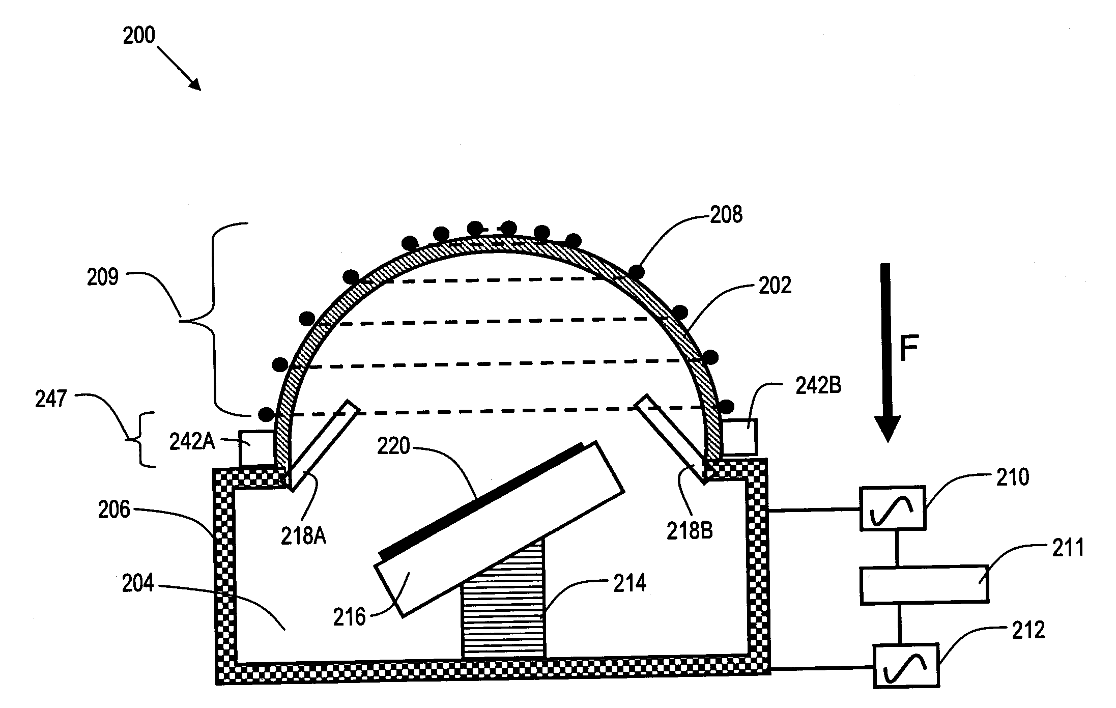
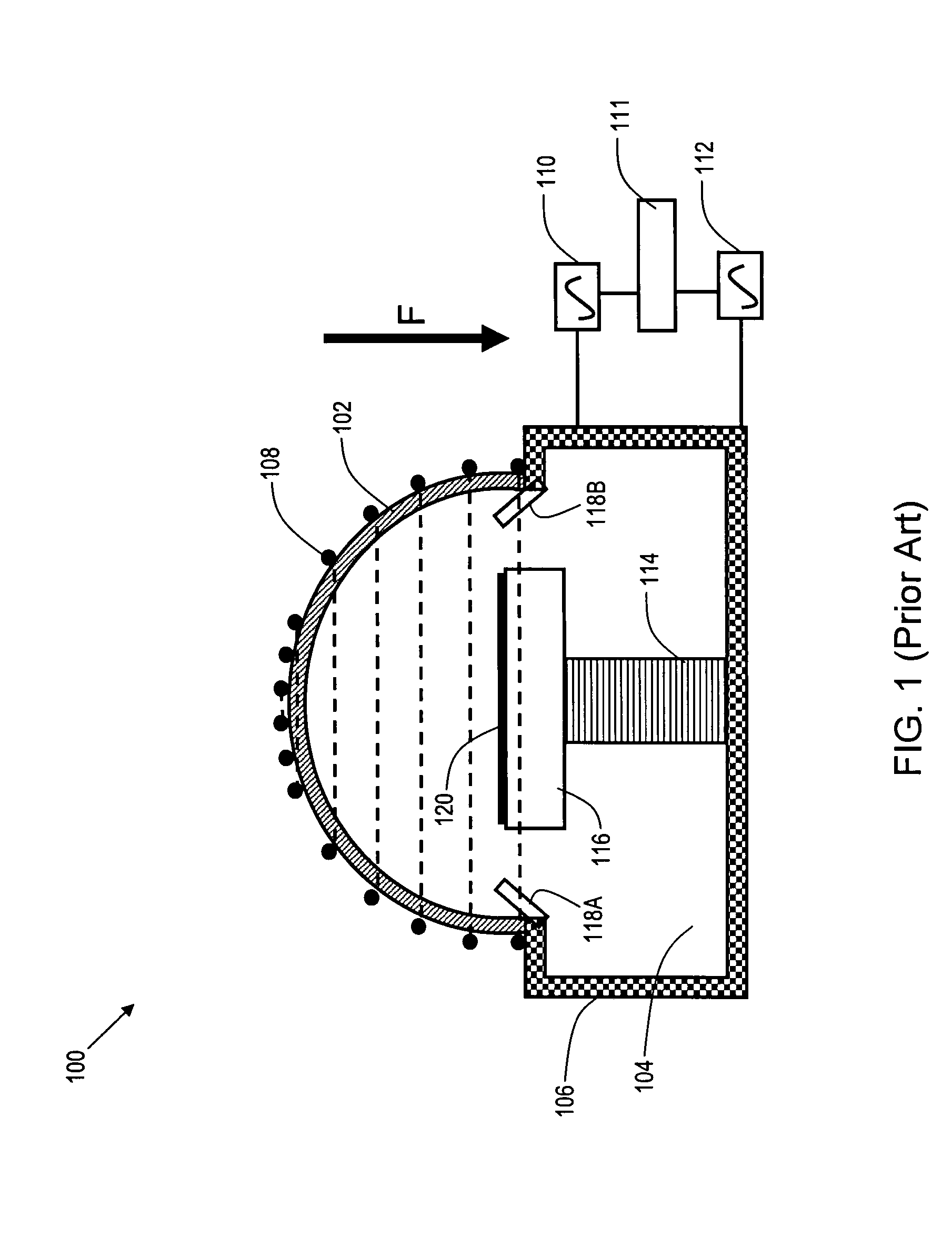
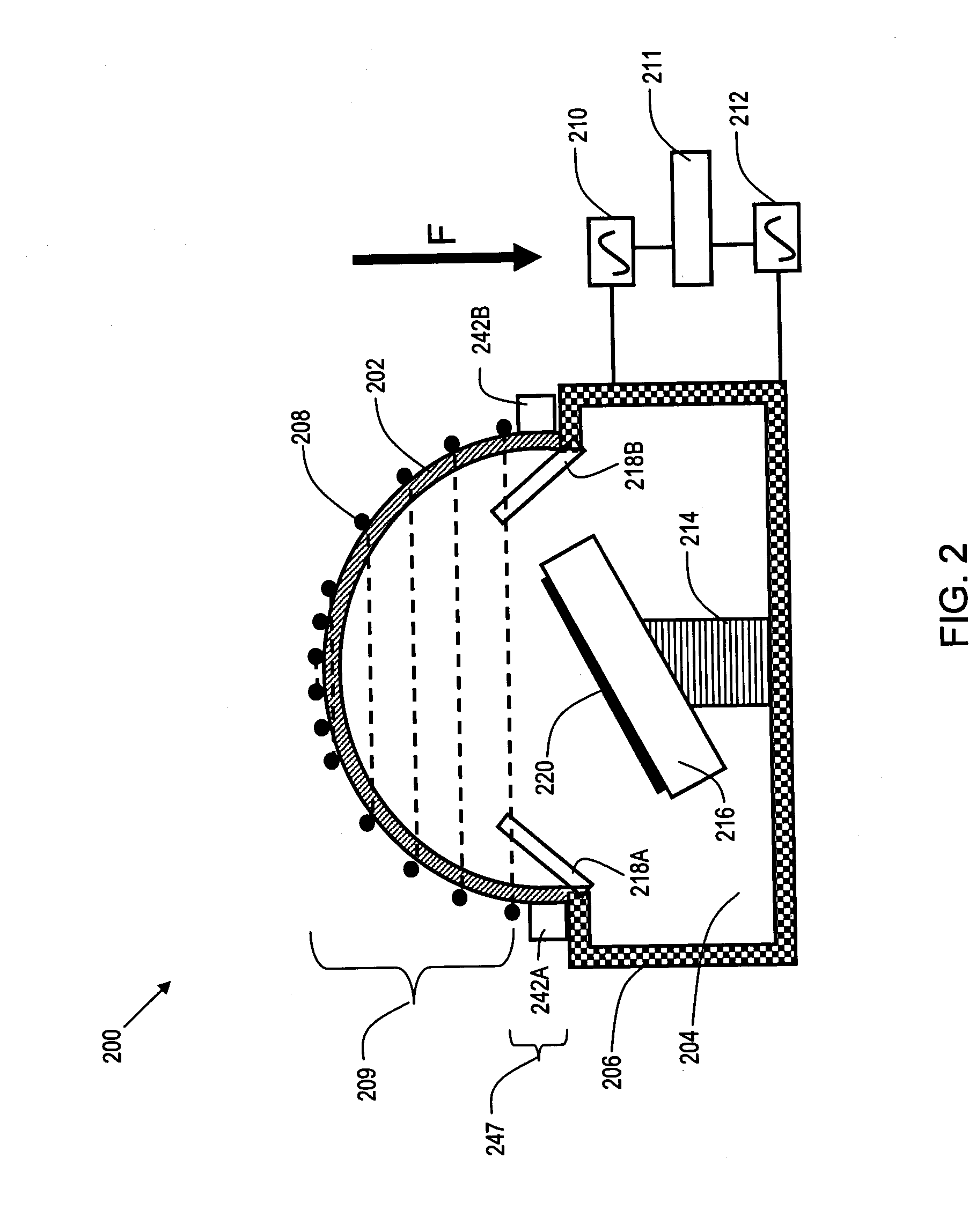
[0053]FIG. 1 shows a prior art plasma chemical vapor deposition (CVD) tool 100. The prior art method will be briefly reviewed here to provide context for discussion of the present invention. Tool 100 comprises a chamber 104. The chamber is comprised of a base section, which is formed by chamber walls 106, and a dome 102. Dome 102 may be comprised of a ceramic material. Disposed around dome 102 is induction coil 108. A column 114 supports a pedestal 116. Pedestal 116 serves to support workpiece 120. Workpiece 120 is typically a semiconductor wafer comprising a plurality of die undergoing fabrication. Pedestal 116 also serves as an electrode in the deposition process. A plurality of gas injectors (shown as 118A and 118B) inject a gas into chamber 104. Frequency source 110 provides a frequency (typically around 400 KHz) that creates a magnetic flux in the chamber 104, in a downward direction (as indicated by arrow F). Frequency source 112 provides a frequency (typically around 13.56 MH...


PUM

PropertyMeasurementUnit
angleaaaaaaaaaa
frequencyaaaaaaaaaa
frequencyaaaaaaaaaa

Abstract

Forming a shallow trench capacitor in conjunction with an FET by forming a plurality of STI trenches; for the FET, implanting a first cell well having a first polarity between a first and a second of the STI trenches; for the capacitor, implanting a second cell well having a second polarity in an area of a third of the STI trenches; removing dielectric material from the third STI trench; forming a gate stack having a first portion located between the first and the second of the STI trenches and a second portion located over and extending into the third trench; and performing a source / drain implant of the same polarity as the second cell well, thereby forming a FET in the first cell well, and a capacitor in the second cell well. The second polarity may be opposite from the first polarity. An additional implant may reduce ESR in the second cell well.

Description

FIELD OF THE INVENTION[0001]The present invention generally relates to the fields of semiconductor fabrication and, more particularly, to high-density plasma (HDP) chemical vapor deposition (CVD) apparatuses and methods of forming semiconductor devices using the same.BACKGROUND OF THE INVENTION[0002]In general, semiconductor manufacturing comprises multiple process steps. As semiconductor integrated circuits (ICs) have continued to increase in complexity, the number of metallization levels, and number of devices on a chip have increased in like manner. Various features within a particular chip often require multiple steps to build. For example, in some cases, multiple lithography, deposition, and planarization steps are required. Each process step adds cost and complexity to the manufacturing process, and may adversely affect overall product yield. It is therefore desirable to reduce the number of process steps required to fabricate a given semiconductor IC.[0003]Features commonly f...

Claims


Application Information

Patent Timeline
Patent Type & Authority Applications(United States)
IPC IPC(8): H01L21/311
CPCC23C16/345C23C16/402C23C16/45578C23C16/4586C23C16/507C23C16/56H01L27/10867H01J37/321H01J2237/20207H01J2237/3323H01L21/31608H01L21/3185H01J37/20H01L21/02274H01L21/02211H01L21/02164H01L21/0217H10B12/0385
Inventor YANG, DAEWONCHENG, KANGGUOSMETANA, PAVELWISE, RICHARD S.WONG, KEITH KWONG HON
Owner ALSEPHINA INNOVATIONS INC
Why Eureka
Try Eureka