Semiconductor memory device for precharging bit lines except for specific reading and writing periods

a memory device and memory technology, applied in the direction of information storage, static storage, digital storage, etc., can solve the problems of data loss, erroneous operation, data loss, etc., and achieve the effect of preventing data-charge loss and improving data holding characteristics

Inactive Publication Date: 2010-04-06
LONGITUDE SEMICON S A R L
View PDF4 Cites 6 Cited by
  • Summary
  • Abstract
  • Description
  • Claims
  • Application Information

AI Technical Summary

Benefits of technology

[0023]In light of the above circumstances, the present invention relates to a DRAM cell whose access transistor is a floating body transistor such as a planar or pillar transistor formed on an SOI substrate, and has an object to provide a semiconductor memory device in which when a bit line is selected, it is possible to prevent data-charge loss in a non-selected memory cell which is also connected to the relevant bit line (similar to the selected memory cell), thereby improving data holding characteristics.
[0057]As described above, in accordance with the present invention, (i) each bit line in a non-selected memory cell (i.e., not selected using a word line) is always precharged so as to have the predetermined precharge voltage, which may be lower than or equal to the L level with respect to the amplitude of the bit line, and (ii) each bit line in a selected memory cell (i.e., by using a word line) is isolated or disconnected from the relevant sense amplifier by the switching device and is precharged so as to have the predetermined precharge voltage (which may be lower than or equal to the L level with respect to the amplitude of the bit line) except for each very short period with respect to data reading and data rewriting (which includes data writing). Therefore, with respect to each DRAM cell whose access transistor is a floating-body transistor such as a planer or pillar transistor formed on an SOI substrate, no electric charge is stored in the relevant floating body, and it is possible to prevent data-charge leakage due to a parasitic bipolar effect or a decrease in a relevant threshold voltage, thereby improving data holding characteristics of the relevant DRAM.
[0058]Also in accordance with the present invention, (i) each local bit line in a non-selected memory cell (i.e., not selected using a word line) is always precharged so as to have the predetermined precharge voltage, which may be lower than or equal to the L level with respect to the amplitude of the bit line, and (ii) each local bit line in a selected memory cell (i.e., by using a word line) is also precharged so as to have the predetermined precharge voltage (which may be lower than or equal to the L level with respect to the amplitude of the bit line) except for each very short period with respect to data reading and data rewriting (which includes data writing). Therefore, with respect to each DRAM cell whose access transistor is a floating-body transistor such as a planer or pillar transistor formed on an SOI substrate, no charge is stored in the relevant floating body, and it is possible to prevent data-charge leakage due to a parasitic bipolar effect or a decrease in a relevant threshold voltage, thereby improving data holding characteristics of the relevant DRAM.

Problems solved by technology

After that, at the instant when the level of the bit-line potential shifts to L (low), a leakage current flows due to a parasitic bipolar action, by which the charge as the data (i.e., data charge) stored in the relevant capacitor is lost, and an erroneous operation such as a data loss occurs.
However, in Patent Document 1, as the body refresh mode is added to the normal operation mode, the operation becomes complex, which thereby increases both the circuit size and the chip area.
Furthermore, as the body refresh is necessary in addition to the normal refresh operation, the busy rate with respect to the access prohibition to a DRAM cell increases, which affects the access time, and also causes deviation from the standard specification, thereby removing compatibility with other DRAMs.
In this case, it is impossible to solve a problem in which at the instant when the period of the page mode access is completed and the relevant bit line is precharged to the “L” potential, a data charge stored in a non-selected memory cell, which has been connected to the precharged bit line, is lost.

Method used


Image

  • Semiconductor memory device for precharging bit lines except for specific reading and writing periods
  • Semiconductor memory device for precharging bit lines except for specific reading and writing periods
  • Semiconductor memory device for precharging bit lines except for specific reading and writing periods

Examples


second embodiment

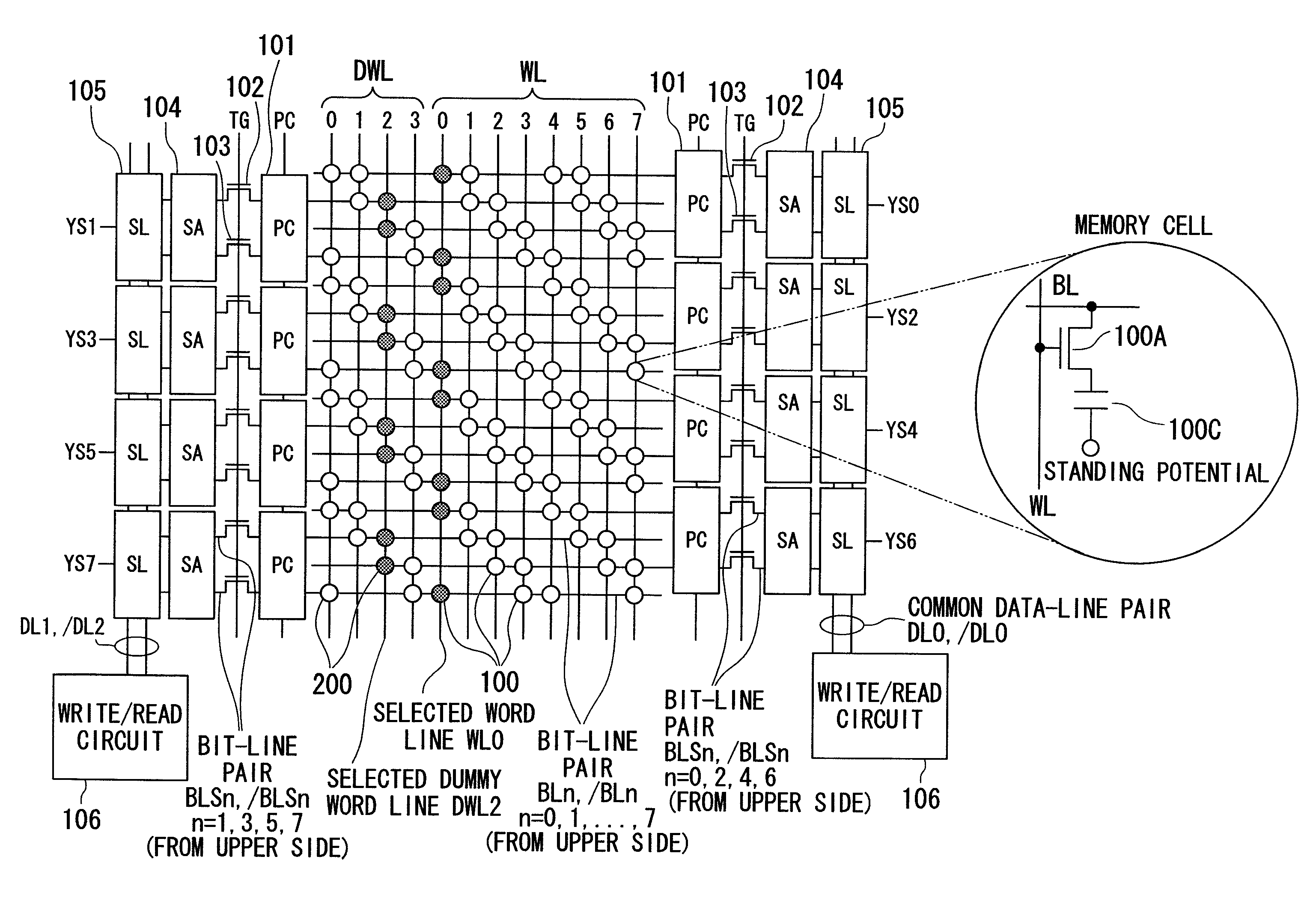
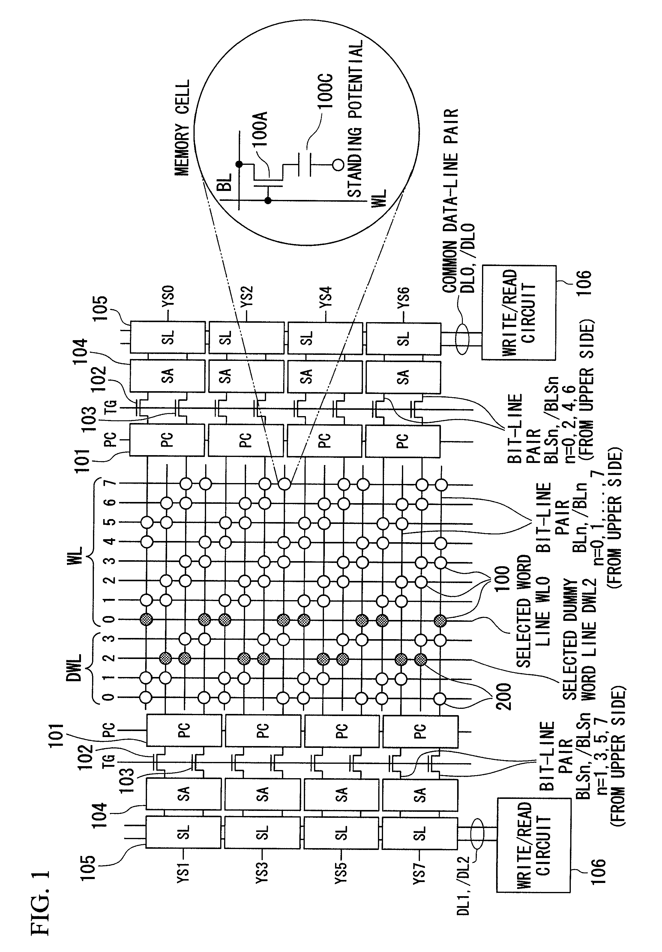
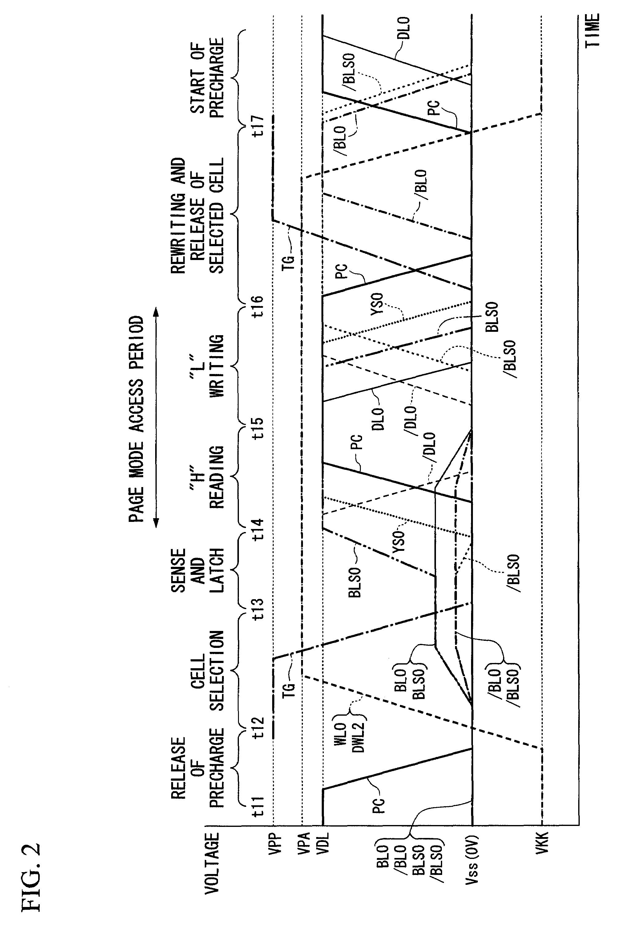
[0162]FIGS. 7 to 9 are diagrams showing the structure of a semiconductor memory device (DRAM memory cell array) as a second embodiment of the present invention.

[0163]FIG. 7 is a diagram showing the general concept of the memory cell array, and shows a hierarchical structure including global bit lines GBLs and local bit lines LBLs, where each bit line is of a single-end type.

[0164]To each local bit line LBL, a local sense amplifier LSA of a single-end input type is connected. On the other hand, to each global bit line GBL, a global sense amplifier GSA of a single-end input type is connected.

[0165]When data is read from each memory cell, a control circuit (for controlling each part of the semiconductor memory device) connects a target local sense amplifier LSA to the relevant global bit line GBL. Accordingly, the local sense amplifier LSA first inverts and amplifies data read from the corresponding local bit line LBL, and transmits the amplified result to the connected global bit line...


PUM


Abstract

A semiconductor memory device includes a memory cell having an FET of a floating body type, and a capacitor for storing a data charge; a bit line to which the source or the drain of the FET is connected; a precharging device for performing precharge control so that the bit line has a predetermined precharge voltage; a sense amplifier for amplifying and storing the potential of the bit line, which is set in accordance with the data charge read from the memory cell; a switching device, provided between the bit line and the sense amplifier, for performing selective connection therebetween; and a control part for controlling the precharging device, the sense amplifier, and the switching device. Except for each period for performing data reading or writing, the control part makes the precharging device perform the precharge control and makes the switching device disconnect the bit line from the sense amplifier.

Description

BACKGROUND OF THE INVENTION[0001]1. Field of the Invention[0002]The present invention relates to a semiconductor memory device, and in particular, those which use an SOI (silicon on insulator) substrate.[0003]Priority is claimed on Japanese Patent Application No. 2007-139105, filed May 25, 2007, the contents of which are incorporated herein by reference.[0004]2. Description of the Related Art[0005]In an SOI substrate which is widely used in semiconductor devices, an (embedded) insulating film is provided on a silicon substrate, and a silicon layer is further provided thereon.[0006]A semiconductor memory device using the above-described SOI and having an FBC (floating body cell) memory cell has been developed, in which a part corresponding to the channel area of a MOS transistor (as a floating-body transistor) formed in a silicon layer on an embedded insulating film is formed as a floating body where a charge as data is stored.[0007]In a DRAM (dynamic random access memory) cell which...

Claims


Application Information

Patent Timeline
Patent Type & Authority Patents(United States)
IPC IPC(8): G11C7/00
CPCG11C11/4094G11C11/4076
Inventor KAJIGAYA, KAZUHIKO
Owner LONGITUDE SEMICON S A R L
Why Eureka
Try Eureka