

Power semiconductor module
a technology of power semiconductor modules and plastic encapsulation, which is applied in the direction of semiconductor devices, semiconductor/solid-state device details, electrical apparatus, etc., can solve the problems of limiting the power range of semiconductor modules, high cost of plastic-encapsulated semiconductor housings, and danger of sagging toward the middle, etc., to achieve good cooling, good heat dissipation, and compact structure
- Summary
- Abstract
- Description
- Claims
- Application Information
AI Technical Summary
Benefits of technology
Problems solved by technology
Method used
Image

Examples
Embodiment Construction
[0004]The object of the invention is therefore to devise a power semiconductor module which has improved cooling relative to the prior art.
[0005]This object is achieved as claimed in the invention by the features of the independent claim 1.
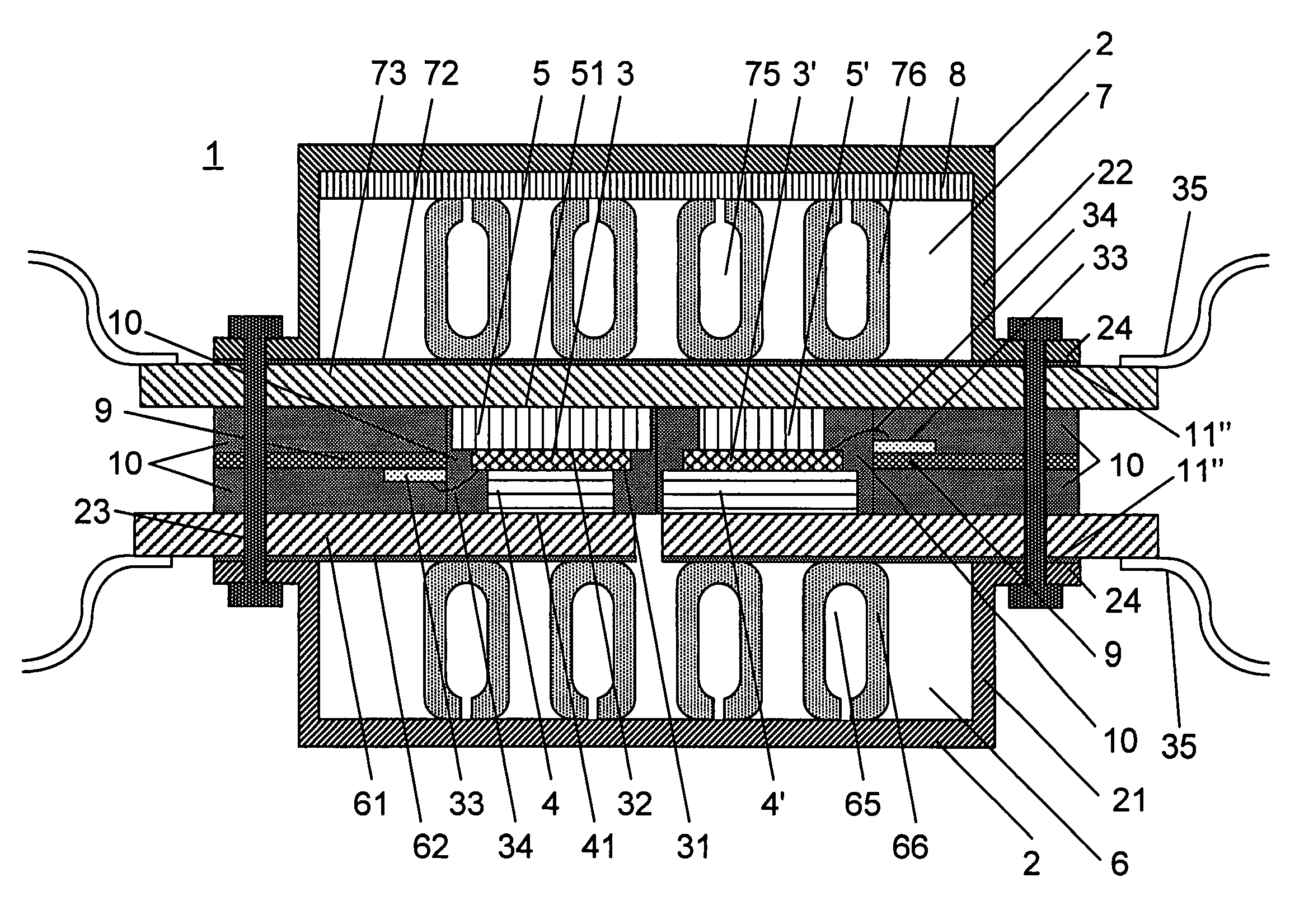
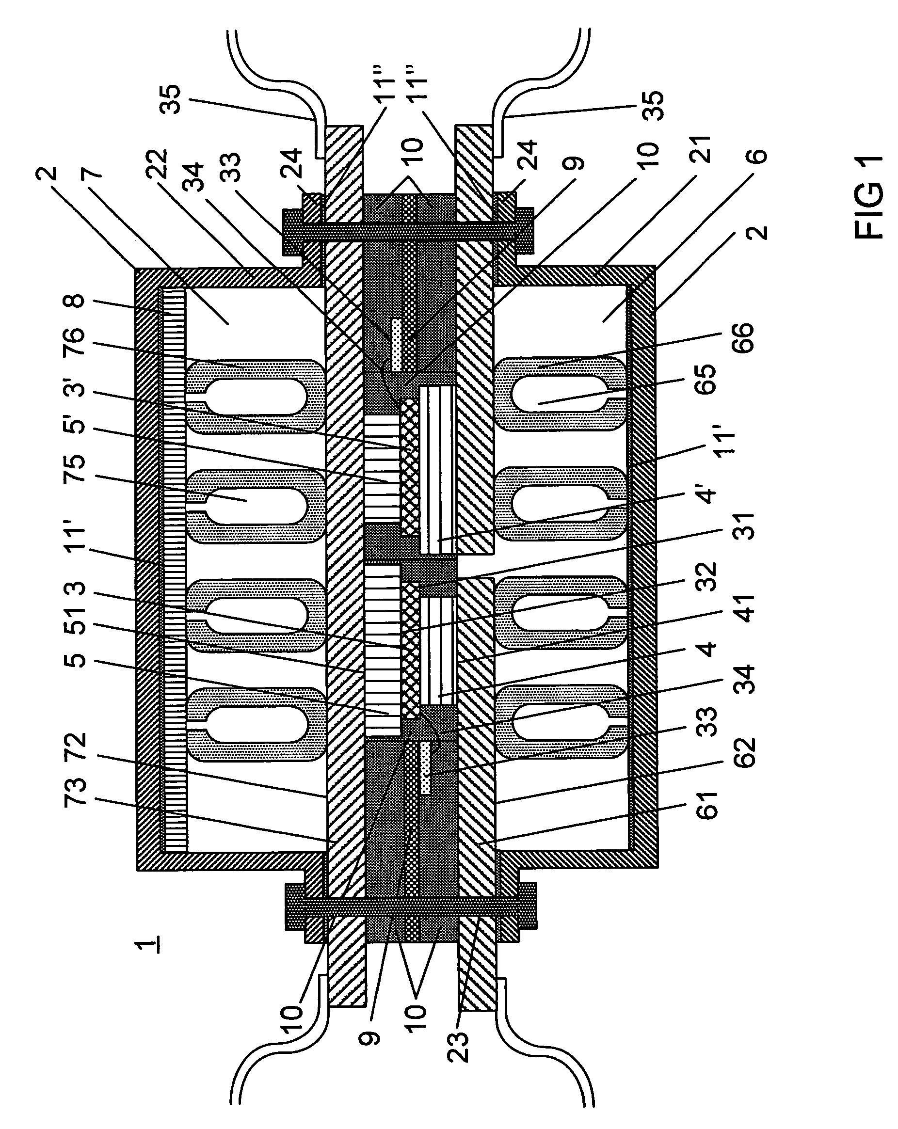
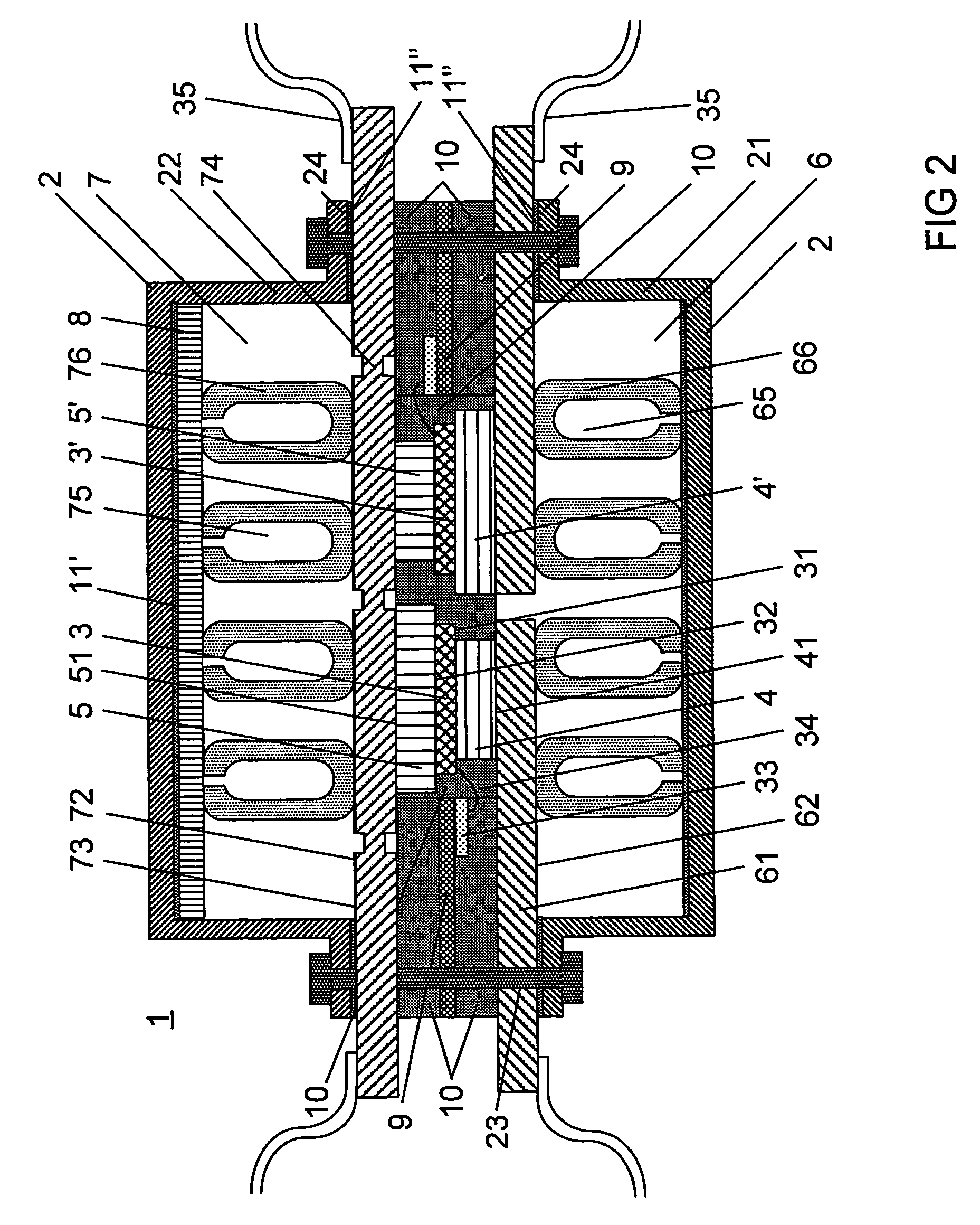
[0006]The power semiconductor module as claimed in the invention has at least one semiconductor chip with a first main electrode side and a second main electrode side opposite the first main electrode side. The first main electrode side makes thermal and electrical contact with the first base plate. This first base plate makes thermal contact with a first cooling device on the side of the first base plate facing away from the first main electrode side. The first cooling device has a first main electrode connecting element and a heat sink, the first main electrode connecting element making thermal and electrical contact with the side of the first base plate facing away from the first main electrode side, and the heat sink making thermal contact wit...
PUM
 Abstract
Description
Claims
Application Information