Method and apparatus for designing semiconductor integrated device using noise current and impedance characteristics of input/output buffers between power supply lines

a technology of noise current and impedance characteristics, applied in the direction of cad circuit design, program control, instruments, etc., can solve the problems of difficult effective reduction of noise current and inability to reduce noise current, so as to achieve effective reduction of noise current and noise current, the effect of reducing noise curren

Inactive Publication Date: 2010-04-13
RENESAS ELECTRONICS CORP
View PDF5 Cites 9 Cited by
  • Summary
  • Abstract
  • Description
  • Claims
  • Application Information

AI Technical Summary

Problems solved by technology

In the above-described prior art semiconductor integrated device designing method, however, since the noise current inherently has a frequency spectrum due to the reflection of signals by load transmission lines (or wiring lines) connected to the input / output buffers or the like derived from the impedance mismatching between the input / output buffers and the load transmission lines, the noise current actually cannot be decreased.
Therefore, even when the resonant frequency of the frequency-to-impedance characteristic curve departs from the operating frequency of the semiconductor integrated device, it is difficult to effectively decrease the noise current.

Method used


Image

  • Method and apparatus for designing semiconductor integrated device using noise current and impedance characteristics of input/output buffers between power supply lines
  • Method and apparatus for designing semiconductor integrated device using noise current and impedance characteristics of input/output buffers between power supply lines
  • Method and apparatus for designing semiconductor integrated device using noise current and impedance characteristics of input/output buffers between power supply lines

Examples


Embodiment Construction

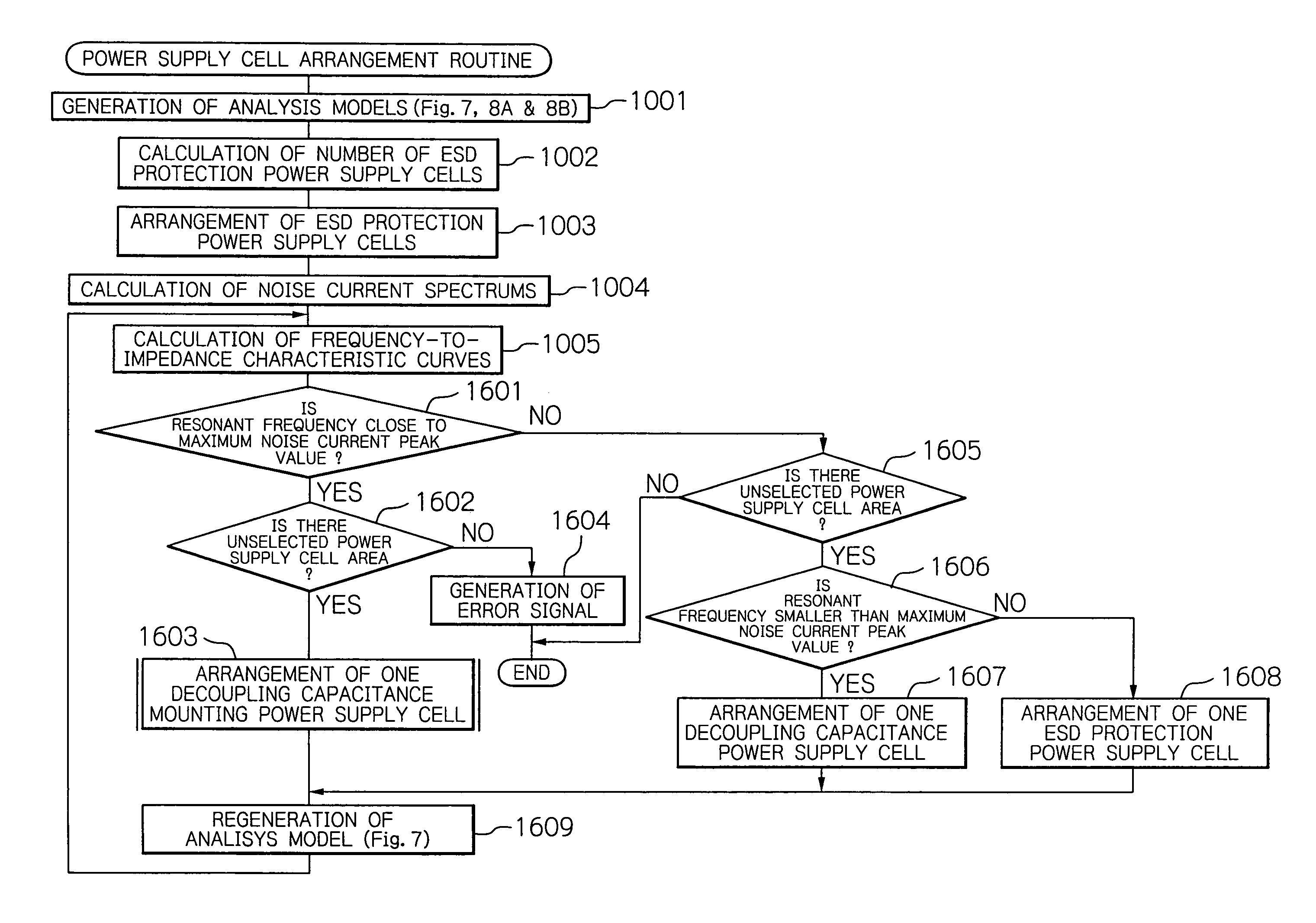
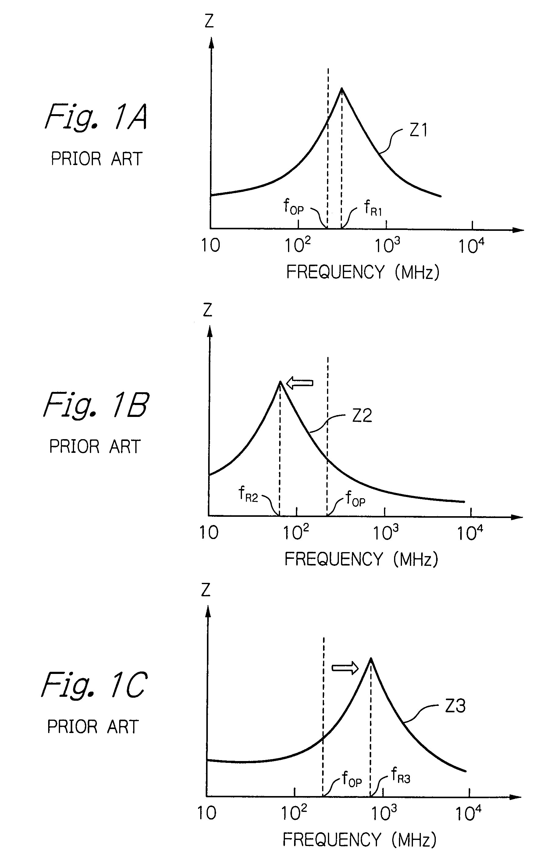
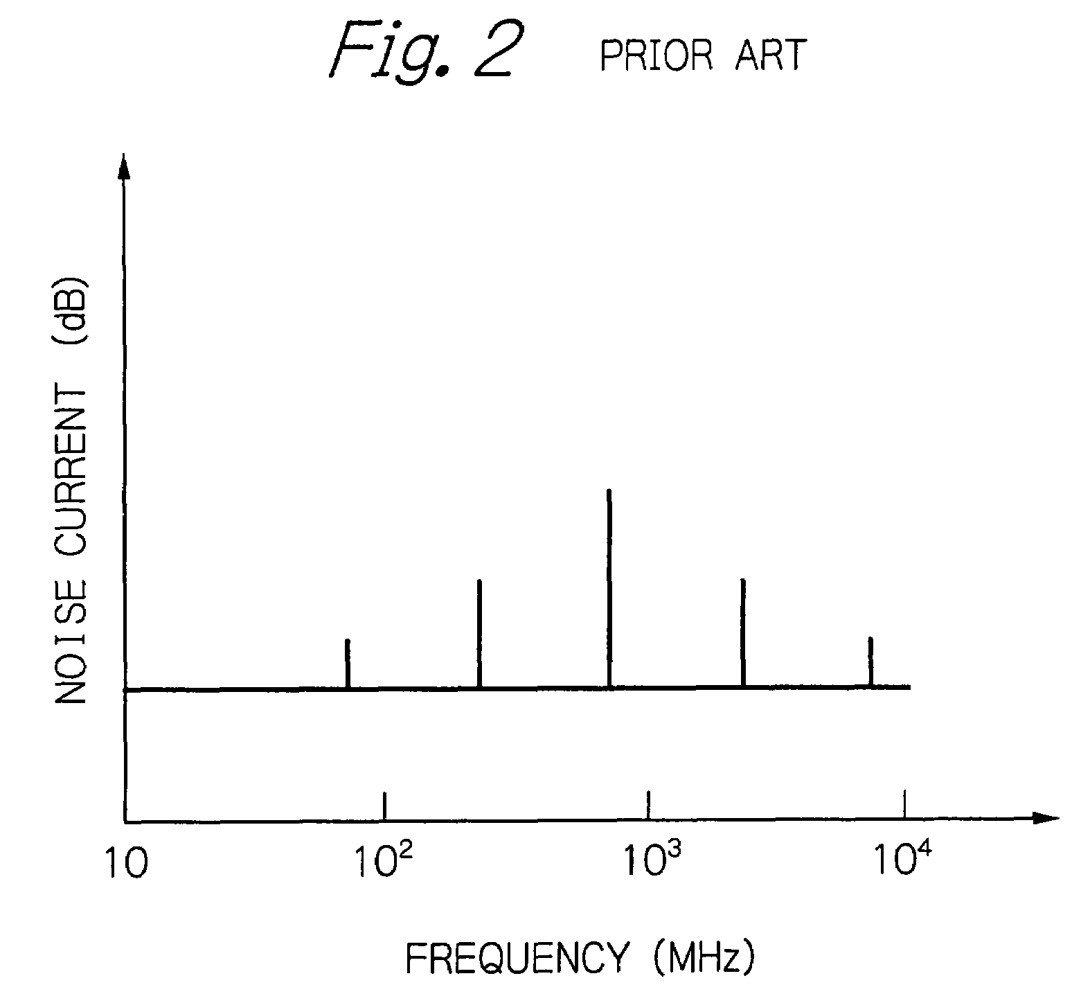
[0032]Before the description of the preferred embodiment, a prior art semiconductor integrated device designing method will be explained with reference to FIGS. 1A, 1B and 1C (see: JP-2005-196406 A).

[0033]First, referring to FIG. 1A, a frequency-to-impedance characteristic curve Z1 between two power supply lines is calculated in accordance with circuit design data for a semiconductor integrated device (chip). In the frequency-to-impedance characteristic curve Z1, the impedance Z is maximum at a frequency which is called a resonant frequency fR1. In this case, the resonant frequency fR1 is very close to the operating frequency fop of the semiconductor integrated device, so that the noise current would be remarkably increased.

[0034]Next, as shown in FIG. 1B, in order to decrease the noise current, the resonant frequency is decreased to fR2 by increasing the inductance and / or capacitance between the power supply lines so that a frequency-to-impedance curve Z2 is obtained. On the other ...


PUM


Abstract

In a method for designing a semiconductor integrated device, there are prepared a first power supply cell having a first decoupling capacitance and a second power supply cell having a second decoupling capacitance larger than the first decoupling capacitance. One of the first and second power supply cells is arranged in each of power supply cell areas of an input / output circuit area of the semiconductor integrated device in accordance with frequency-to-impedance characteristics at a predetermined point of input / output buffers of the input / output circuit area between first and second power supply lines thereof and frequency-to-noise current characteristics of the input / output buffers of the input / output circuit area between the first and second power supply lines.

Description

BACKGROUND OF THE INVENTION[0001]1. Field of the Invention[0002]The present invention relates to a method and apparatus for designing a semiconductor integrated device, and more particularly, to a method and apparatus for arranging power supply cells in an input / output circuit area of the semiconductor integrated device.[0003]2. Description of the Related Art[0004]Generally, a semiconductor integrated device is partitioned by an internal circuit area and an input / output circuit area surrounding the internal circuit area. The input / output circuit area includes power supply cells and input / output buffers.[0005]The power supply cells receive power supply voltages via pads from the exterior and supply the power supply voltages via power supply lines to the input / output buffers as well as the internal circuit area.[0006]The input / output buffers are connected via pads to external devices, so that the input / output buffers carry out signal transmission between the semiconductor integrated d...

Claims


Application Information

Patent Timeline
Patent Type & Authority Patents(United States)
IPC IPC(8): G06F17/50
CPCG06F17/5068G06F17/5036G06F30/367G06F30/39
Inventor MASUMURA, YOSHIHIRO
Owner RENESAS ELECTRONICS CORP
Why Eureka
Try Eureka