Method for forming MOS transistor

a metaloxide semiconductor and transistor technology, applied in transistors, basic electric elements, electrical equipment, etc., can solve the problems of generating considerable interstitial defects, reducing the lateral diffusion and ted effect of the first dopant, and affecting the effect of the formation depth control

Active Publication Date: 2010-04-20
UNITED MICROELECTRONICS CORP
View PDF9 Cites 19 Cited by
  • Summary
  • Abstract
  • Description
  • Claims
  • Application Information

AI Technical Summary

Benefits of technology

[0010]Therefore the present invention provides a method for forming a MOS transistor capable of reducing a TED effect and a short channel effect.
[0014]Because the co-implantation process is performed before the PAI process, before the first ion implantation process, or after the first ion implantation process, the lateral diffusion and TED effect of the first dopant are reduced. The present invention thus provides a method for forming MOS transistor capable of controlling diffusion of the first dopant, providing a good junction profile, and reducing a short channel effect.

Problems solved by technology

However, a short channel effect, which results in a poor threshold voltage roll-off characteristic, always accompanies miniaturization.
However, as device scale is reduced to 90-nm and smaller, the conventional ultra shallow junction formation hits a limitation in depth control, and co-implantation performed in cooperation with pre-amorphization (PAI) and laser annealing seems to be able to satisfy demands down to 65-nm and even 45-nm processes.
During the ion implantation process, considerable interstitial defects are created because the implanting ion causes damage to a silicon lattice.
TED effect not only deepens the junction profile, but also makes the distribution of the dopant not sheer in a lateral direction, resulting in a severe short channel effect.
However, because the co-implant dopant is vertically implanted into the substrate 100, its control over lateral diffusion of the p-dopant is not fully satisfactory.

Method used


Image

  • Method for forming MOS transistor
  • Method for forming MOS transistor
  • Method for forming MOS transistor

Examples


Embodiment Construction

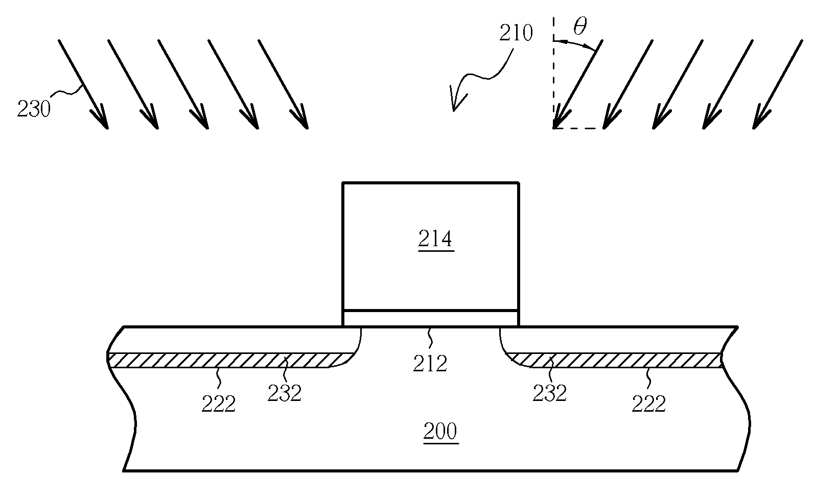
[0021]Please refer to FIGS. 4-8, which are schematic drawings illustrating a first preferred embodiment provided by the present invention. As shown in FIG. 4, a substrate 200 is provided. The substrate 200 comprises a semiconductor wafer, or a silicon-on-insulator (SOI) wafer, etc. The substrate 200 has completely undergone a shallow trench isolation (STI) process and a well formation process, and at least a gate structure 210 having a gate dielectric layer 212 and a gate 214 is formed on the substrate 200. Then a vertical or angled pre-amorphization (PAI) process 220 is performed to form amorphized regions 222 in the substrate 200 adjacent to two sides of the gate structure 210.

[0022]Please refer to FIG. 5. A co-implantation process 230 is subsequently performed to implant a co-implant dopant 232 into the amorphized regions 222. It is noteworthy that the co-implantation process 230 is an oblique angle implantation process and that an angle θ used in the process is in a range from 0...


PUM


Abstract

A method for forming a MOS transistor includes providing a substrate having at least a gate structure formed thereon, performing a pre-amorphization (PAI) process to form amorphized regions in the substrate, sequentially performing a co-implantation process, a first ion implantation process, and a first rapid thermal annealing (RTA) process to form lightly doped drains (LDDs), forming spacers on sidewalls of the gate structure, and forming a source / drain.

Description

BACKGROUND OF THE INVENTION[0001]1. Field of the Invention[0002]The present invention relates to a method for forming metal-oxide semiconductor (MOS) transistor, and more particularly, to a method for forming MOS transistor capable of effectively improving a transient enhanced diffusion (TED) effect and a short channel effect.[0003]2. Description of the Prior Art[0004]With progress in the semiconductor industry, performance and economic factors of integrated circuit design and manufacture have caused a scale of devices in integrated circuits to be drastically reduced to miniaturized sizes, increasing density on a chip. However, a short channel effect, which results in a poor threshold voltage roll-off characteristic, always accompanies miniaturization. To avoid this problem, the prior art has provided a method for forming lightly doped drains (LDDs) having an ultra shallow junction as a solution.[0005]In a conventional ultra shallow junction formation, a low energy ion implantation ...

Claims


Application Information

Patent Timeline
Patent Type & Authority Patents(United States)
IPC IPC(8): H01L21/336
CPCH01L21/26506H01L29/6659H01L21/324H01L21/26586H01L21/26513
Inventor LEE, KUN-HSIENHUANG, CHENG-TUNGTING, SHYH-FANNHUNG, WEN-HANJENG, LI-SHIANCHENG, TZYY-MING
Owner UNITED MICROELECTRONICS CORP
Why Eureka
Try Eureka