Organic Light Emitting Display Device

a light-emitting display and organic technology, applied in the direction of static indicating devices, organic semiconductor devices, instruments, etc., can solve the problems of low transmittivity of organic light-emitting devices, low tft, and the wiring described above, and achieve the effect of increasing outcoupling efficiency and increasing transmittivity

Active Publication Date: 2011-08-25
SAMSUNG DISPLAY CO LTD
View PDF36 Cites 60 Cited by
  • Summary
  • Abstract
  • Description
  • Claims
  • Application Information

AI Technical Summary

Benefits of technology

[0012]The present invention provides a transparent organic light emitting display device having a transmission area with increased transmittivity and increased outcoupling efficiency during double-sided light emission.

Problems solved by technology

In addition, even when the organic light emitting display device is a transparent display device, the transmittivity of the organic light emitting device, the TFT, and the wirings described above is not high, and the spaces between them are very small.
Also, the user may see a distorted image due to the patterns described above, that is, the organic light emitting device, the TFT, and the wirings.
However, since the reflective anode cannot be used in the both emission type display device, optical resonance effects may not be used, which makes it difficult to obtain a high outcoupling efficiency.
Thus, it is difficult to manufacture a transparent organic light emitting display device.

Method used


Image

  • Organic Light Emitting Display Device
  • Organic Light Emitting Display Device
  • Organic Light Emitting Display Device

Examples


Embodiment Construction

[0040]The present invention will now be described more fully with reference to the accompanying drawings, in which exemplary embodiments of the invention are shown.

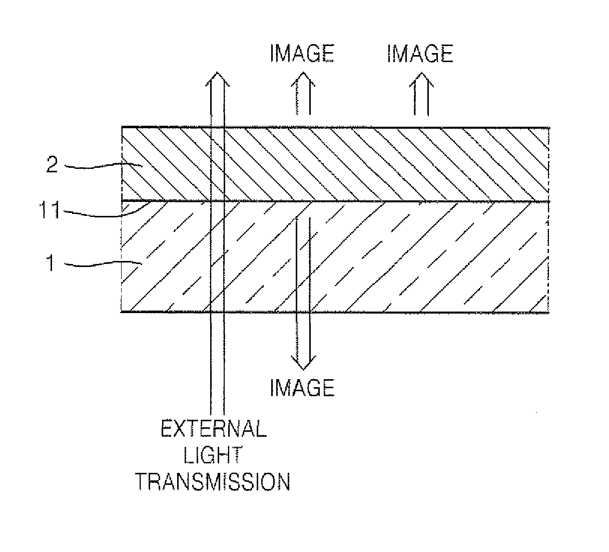
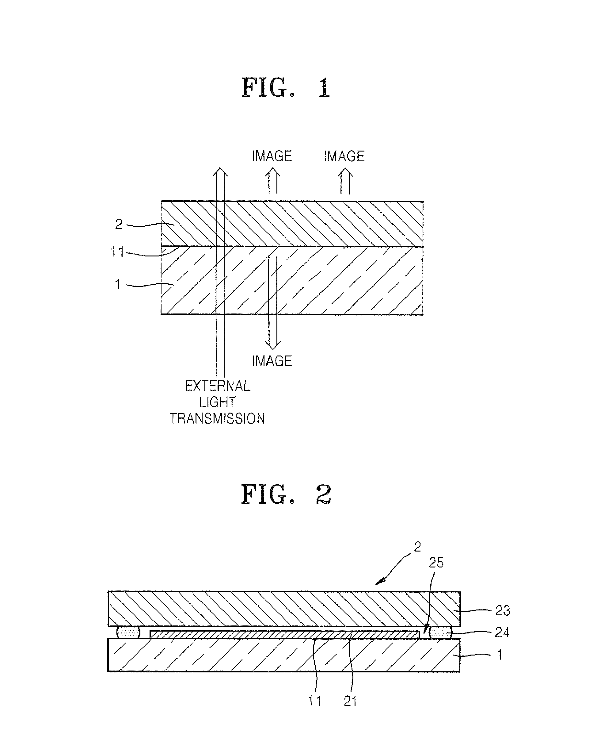
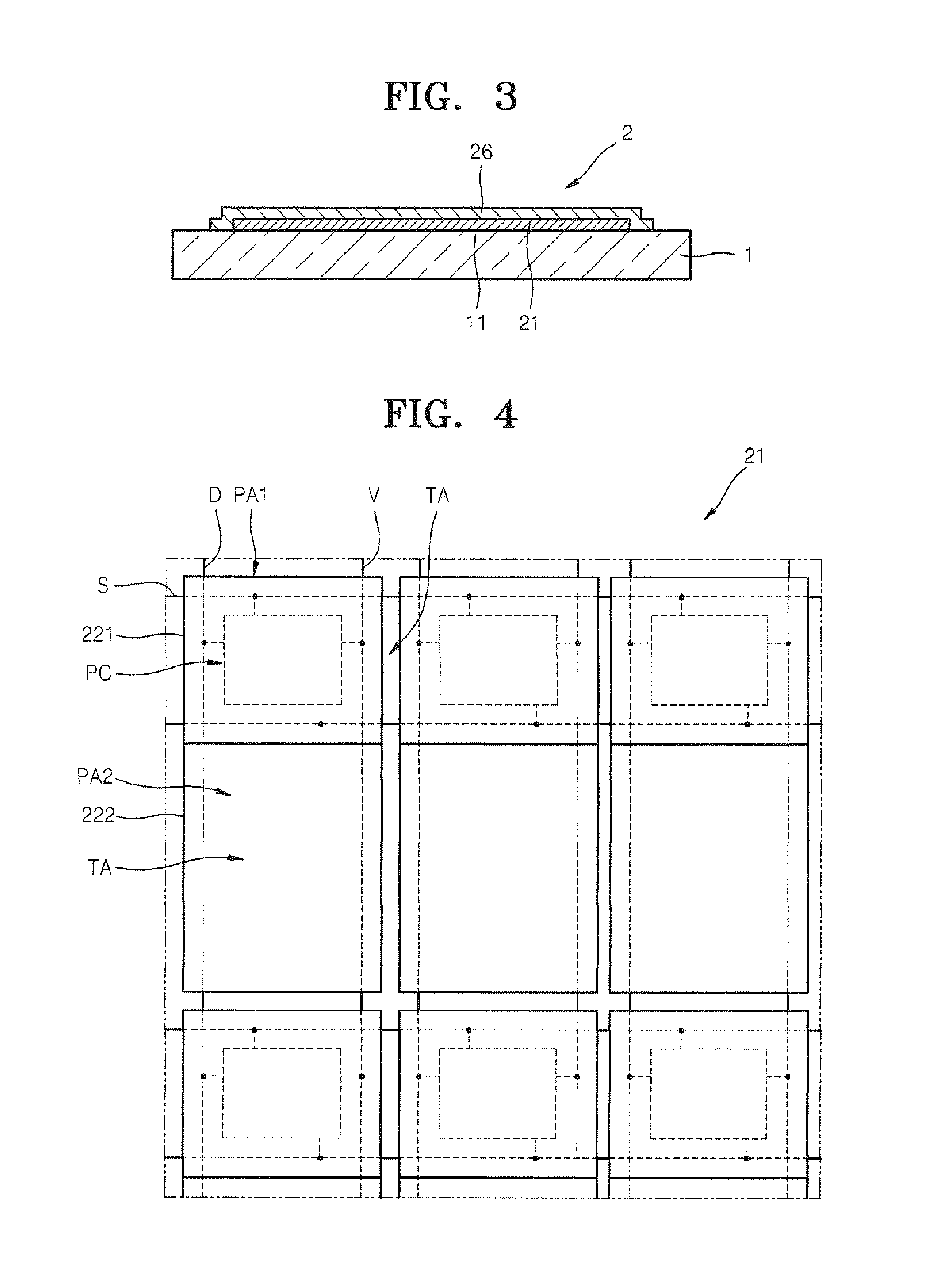
[0041]FIG. 1 is a cross-sectional view illustrating an organic light emitting display device according to an embodiment of the present invention.

[0042]Referring to FIG. 1, the organic light emitting display device includes a substrate 1 and a display unit 2 formed on a first surface 11 of the substrate 1.

[0043]In the above-described organic light emitting display device, external light transmits through the substrate 1 and the display unit 2. The display unit 2 is a both emission type light emitting unit, meaning an image is realized on two surfaces, as shown in FIG. 1.

[0044]The display unit 2 is formed such that external light may be transmitted therethrough as will be described later. Referring to FIG. 1, from a side where an image is formed, the user may view an image formed on an external lower surface of the substrat...


PUM


Abstract

An organic light emitting display device comprises: a substrate; a plurality of thin film transistors (TFTs) formed on a first surface of the substrate; a passivation layer covering the plurality of TFTs; a plurality of first pixel electrodes formed on the passivation layer and respectively electrically connected to the plurality of TFTs, and overlapping with the plurality of TFTs so as to cover the plurality of TFTs, and including a reflection layer formed of a light-reflecting conductive material; a second pixel electrode formed of a light-transmitting conductive material and disposed on the passivation layer so as to be electrically connected to the plurality of first pixel electrodes; an opposite electrode formed such that light is transmitted or reflected therethrough, and disposed opposite the plurality of first pixel electrodes and the second pixel electrode; and an organic layer interposed between the plurality of first pixel electrodes and the second pixel electrode, and including an emission layer. Accordingly, transmittivity of the organic light emitting display device is increased, and optical outcoupling efficiency of the organic light emitting display device is also increased during double-sided emission.

Description

CLAIM OF PRIORITY[0001]This application makes reference to, incorporates the same herein, and claims all benefits accruing under 35 U.S.C. §119 from an application earlier filed in the Korean Intellectual Property Office on the 24th of Feb. 2010 and there duly assigned Serial No. 10-2010-0016665.BACKGROUND OF THE INVENTION[0002]1. Field of the Invention[0003]The present invention relates to an organic light emitting display device and, more particularly, to a transparent organic light emitting display device.[0004]2. Description of the Related Art[0005]Organic light emitting display devices have excellent characteristics in terms of angle of view, contrast, response speed, and power consumption, and thus are widely used in personal portable appliances such as MP3 players or mobile phones and TVs.[0006]The organic light emitting display devices have self-emissive characteristics, and thus do not require a light source, unlike a liquid crystal display (LCD) device which does require a...

Claims


Application Information

Patent Timeline
Patent Type & Authority Applications(United States)
IPC IPC(8): G09G3/32G06F3/038H05B44/00
CPCH01L27/3258H01L27/326H01L27/3276H01L51/5203H01L2251/5323H01L51/5218H01L51/5265H01L2251/5315H01L51/5206H10K59/124H10K59/121H10K59/131H10K50/81H10K50/813H10K50/818H10K50/852H10K2102/3031H10K2102/3026H10K59/805H10K50/805H10K50/84
Inventor JEONG, HEE-SEONGKOH, SUNG-SOOJEONG, CHUL-WOOPARK, SOON-RYONGAN, CHI-WOOKKO, MOO-SOONKIM, OK-BYOUNGJUNG, WOO-SUKCHO, II-RYONGKIM, TAE-KYULEE, DUK-JIN
Owner SAMSUNG DISPLAY CO LTD
Why Eureka
Try Eureka