Method for sealing organic electroluminescence elements and manufacturing method for light emitting panel and display panel
a technology of organic electroluminescence elements and manufacturing methods, which is applied in the manufacture of electrode systems, discharge tubes luminescnet screens, instruments, etc., can solve the problems of reducing the display quality of organic el display panels, deteriorating light emitting properties, and lowering display quality, so as to prevent the reduction of light emitting properties and reliability of light emitting portions or display portions, the effect of high display quality
- Summary
- Abstract
- Description
- Claims
- Application Information
AI Technical Summary
Benefits of technology
Problems solved by technology
Method used
Image
Examples
embodiment 1
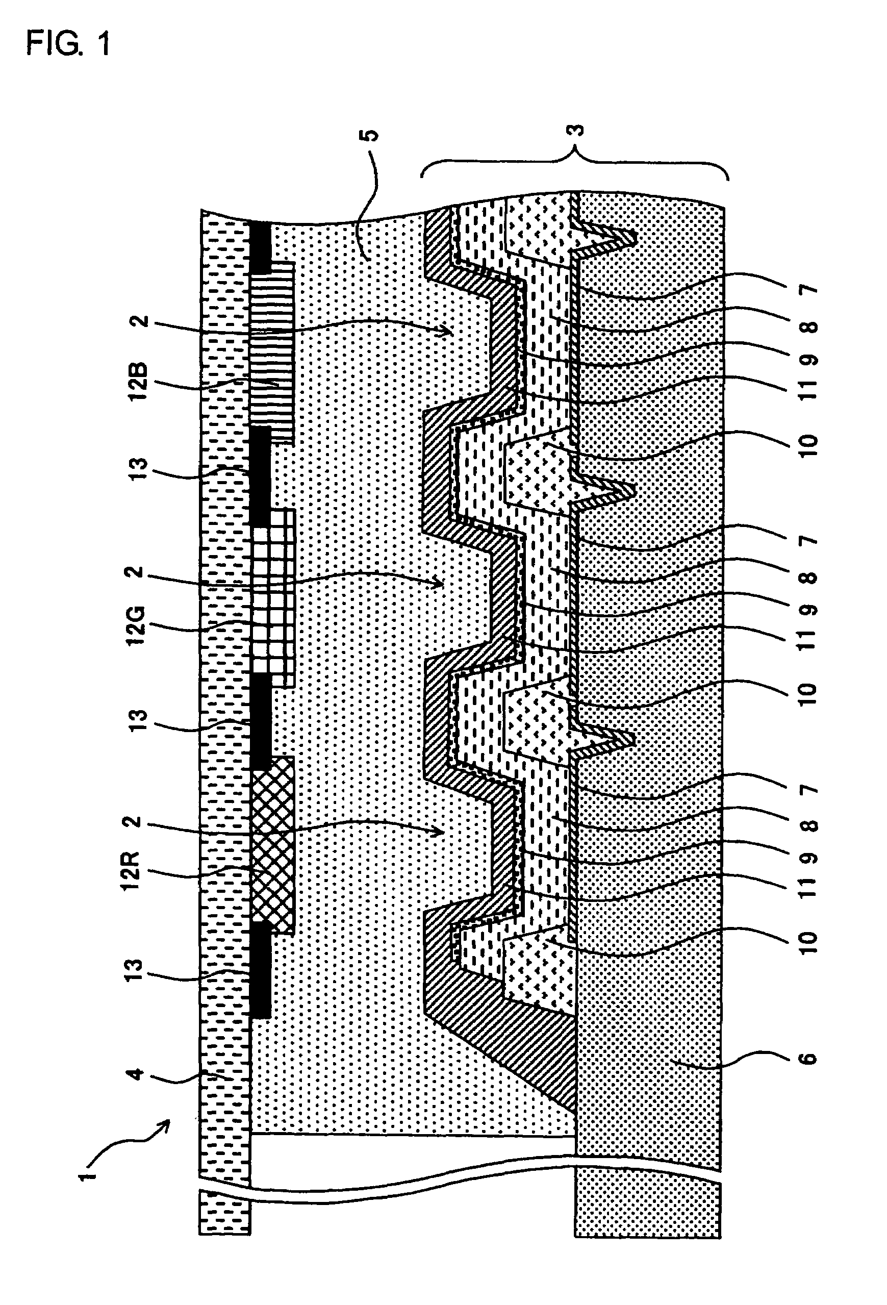
[0096]First, the structure of an organic EL panel that is fabricated using the sealing method according to the present embodiment is described in reference to the schematic cross sectional diagram of FIG. 1.
[0097]1-1. Configuration of Entirety of Organic EL Panel
[0098]FIG. 1 is a schematic cross sectional diagram illustrating the configuration of an organic EL panel that has been fabricated using the sealing method according to the present embodiment.
[0099]In reference to FIG. 1, an organic EL panel 1 is formed by making an organic EL substrate 3 and a sealing substrate 4 for sealing adhere to each other by means of an adhesive 5 for sealing.
[0100]The organic EL substrate 3 is formed of a plurality of organic EL elements 2, 2 . . . which are placed on a TFT substrate 6 on which TFT's for driving are placed.
[0101]In addition, the sealing substrate 4 is formed of a translucent material having color filters 12R, 12G and 12B for red (R), green (G) and blue (B) on the surface facing the ...
embodiment 2
[0128]Next, Embodiment 2 of the present invention is described.
[0129]First, the structure of an organic EL panel that has been fabricated using the sealing method according to the present embodiment is described in reference to the schematic cross sectional diagram shown in FIG. 10.
[0130]2-1. Configuration of Entirety of Organic EL Panel
[0131]FIG. 10 is a schematic cross sectional diagram illustrating the configuration of an organic EL panel that has been fabricated using the sealing method according to the present embodiment.
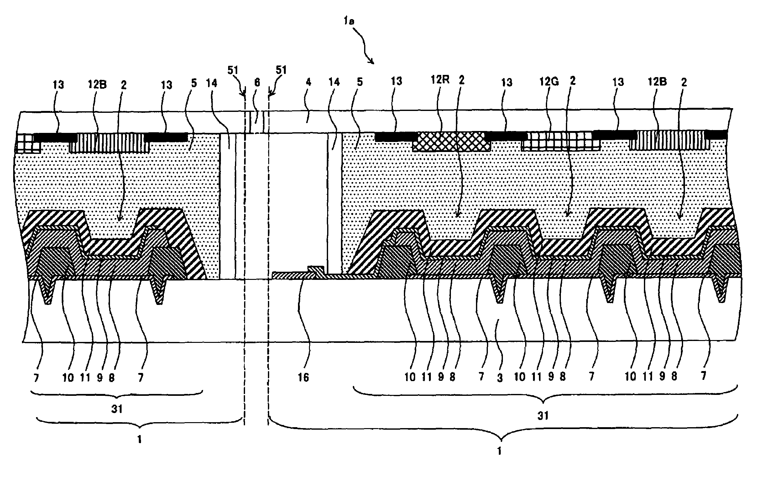
[0132]In reference to FIG. 10, an organic EL panel 20 is formed in such a manner that an organic EL substrate 3 and a sealing substrate 4 for sealing are made to adhere to each other with a first adhesive 14 and a second adhesive 15 for sealing.
[0133]The organic EL substrate 3 is formed of a plurality of organic EL elements 2, 2 . . . , an external circuit which is electrically connected to these organic EL elements 2, and a terminal portion 16 for sending an e...
example 1
[0160]In the following, an example of an organic EL panel 1 that has been fabricated in accordance with a sealing method of the above described Embodiment 1 is described.
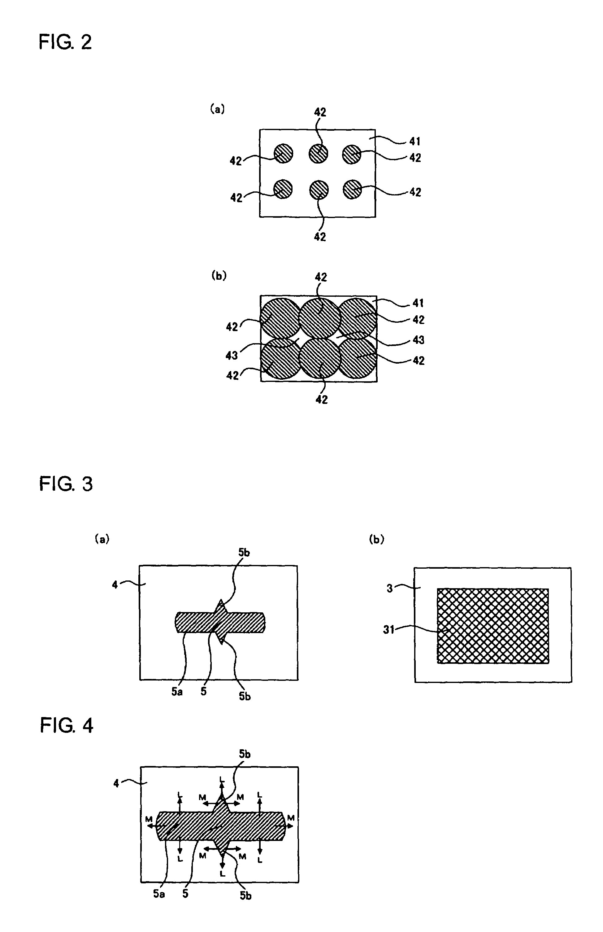
[0161]Organic EL elements 2, 2 . . . were formed on a TFT substrate 6, and thereby, an organic EL substrate 3 was fabricated. FIG. 16(a) is a top plan diagram schematically showing a state where an adhesive 5 has been applied to the surface of a sealing substrate 4. Here, in FIG. 16(a), two directions which are perpendicular to each other are referred to as direction X and direction Y. The direction X and the direction Y are directions parallel to the surface of the sealing substrate 4. The dimensions of this sealing substrate 4 are 40 mm in the longitudinal direction×45 mm in the lateral direction. In addition, FIG. 16(b) is a top plan diagram schematically showing the organic EL substrate 3 and the location of the region of a pixel portion 31 that has been formed on the surface of the organic EL substrate. The dim...
PUM
 Abstract
Description
Claims
Application Information


