Scanning circuit of image sensor

a scanning circuit and image sensor technology, applied in the field of scanning circuits, can solve the problems of variable reading of pixel sensor signals, significant increase in power consumption of image sensors, and image sensors that cannot at high speed read respective pixel signals, and achieve the effect of stable reading of pixel signals and high speed

Inactive Publication Date: 2010-05-04
HONDA MOTOR CO LTD
View PDF8 Cites 0 Cited by
  • Summary
  • Abstract
  • Description
  • Claims
  • Application Information

AI Technical Summary

Benefits of technology

[0014]Accordingly, an object of the present invention is to provide a scanning circuit for reading out light sensor (pixel) signals from an image sensor using light sensor circuits each representing a unit pixel and being capable of producing a pixel light sensor signal corresponding to an photocurrent flowing in a photoelectric converting element, which scanning circuit is capable of stably reading pixel signals at a high speed by using a simple means of saturating each of the light sensor signals by previously turning on respective light sensor circuits, thereby eliminating the need of providing buffer circuits for temporally storing respective pixel signals and / or two shift registers for alternately reading respective pixel signals with a delay from each other.

Problems solved by technology

The above-mentioned image sensor however involves such a problem that, when switches SW11-SW14 were turned on to read respective sensor signals Vo from the respective pixels, it takes time for a voltage signal to rise to a value specified by the bias circuit 7 due to a small current capacity of the output transistor Q3 for each pixel, thereby causing variations in pixel sensor signals read in a time series from respective pixels.
As the result of this, the image sensor cannot at high speed read respective pixel signals.
A drawback of this attempt is that it is accompanied by a significant increase in power consumption of the image sensor because of turning on all buffer amplifiers BF1-BF4.

Method used


Image

  • Scanning circuit of image sensor
  • Scanning circuit of image sensor
  • Scanning circuit of image sensor

Examples


Embodiment Construction

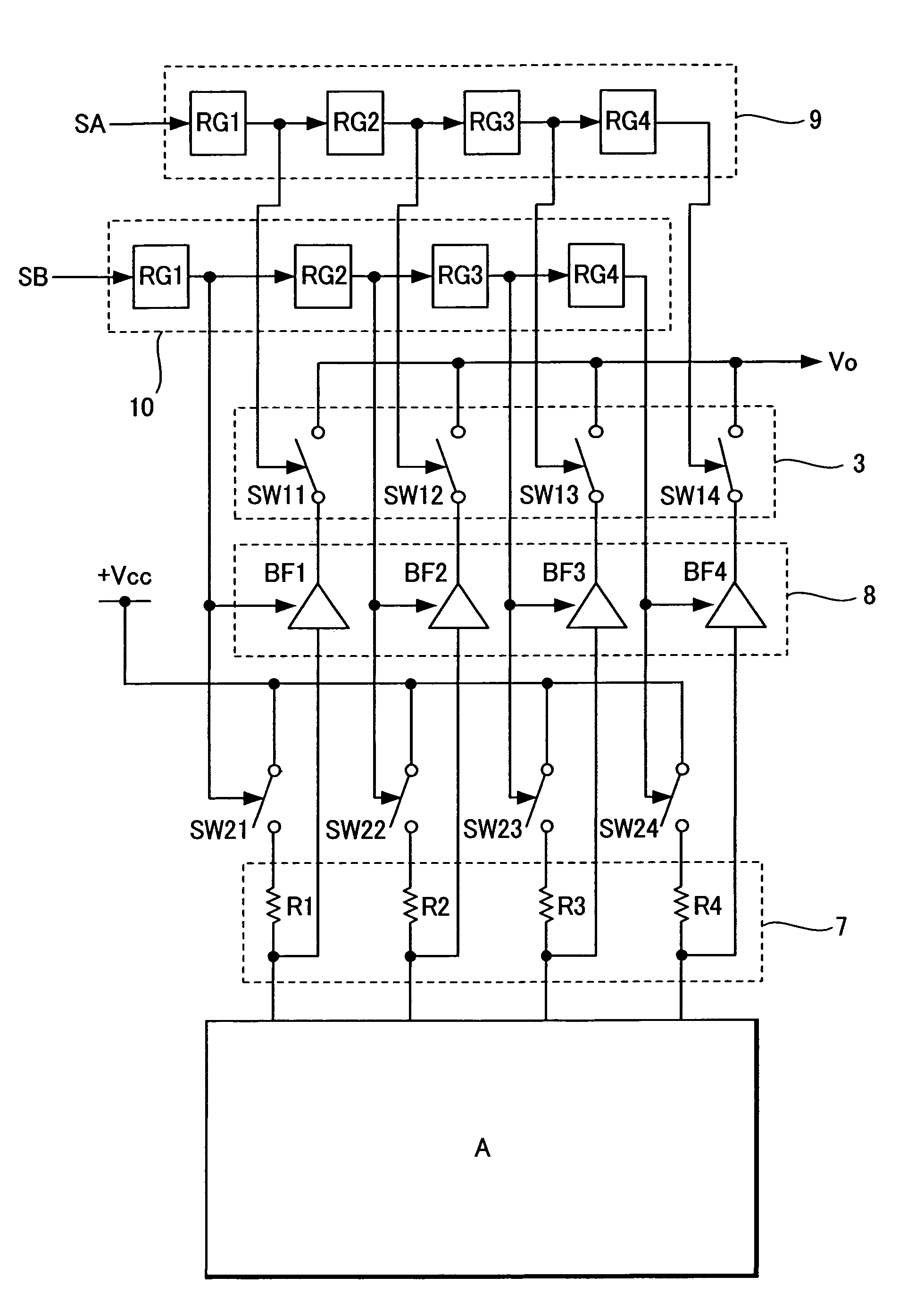
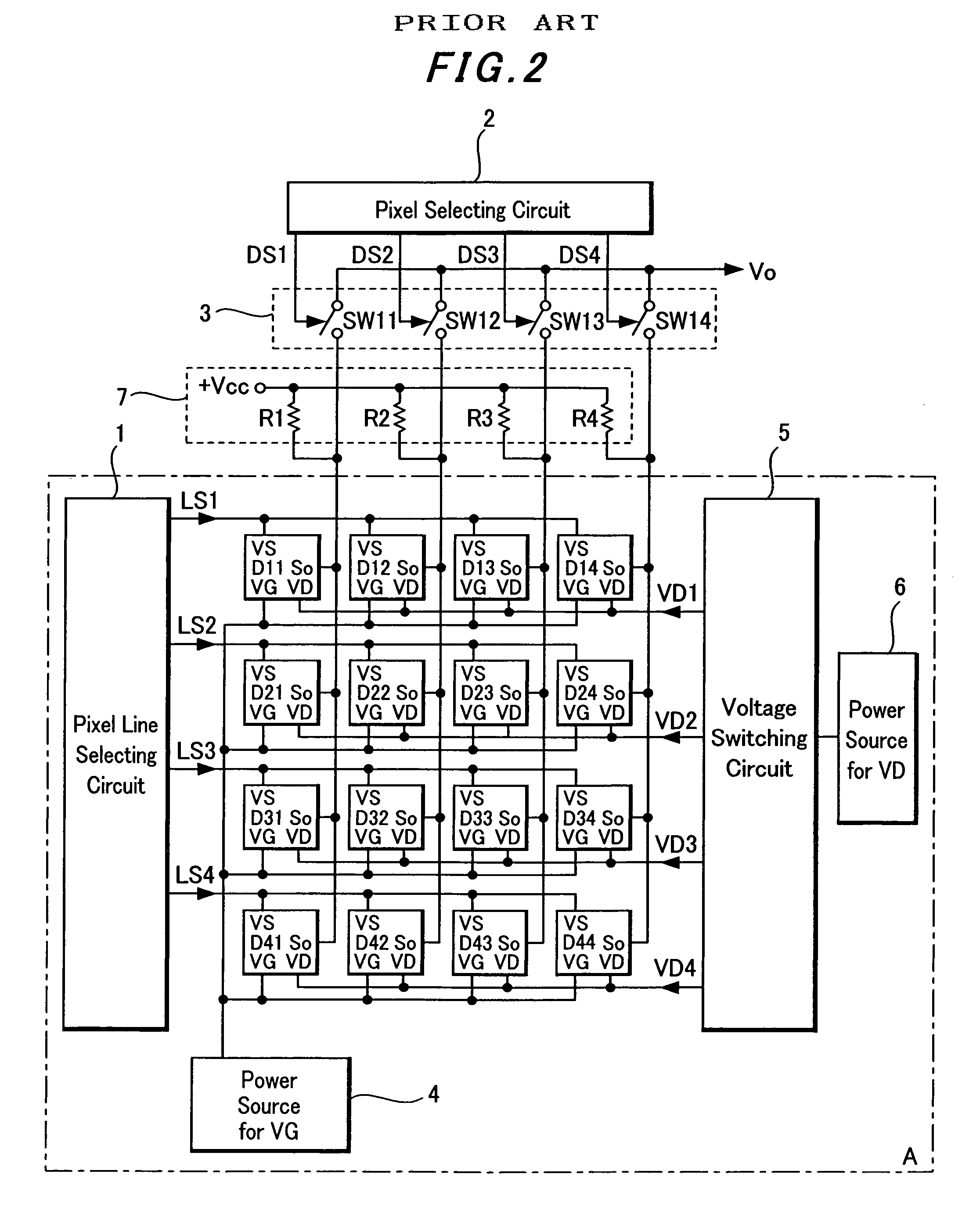
[0032]In an image sensor constructed as shown in FIG. 2, a scanning circuit according to the present invention comprises switches SW21-SW24 connected in series with reference resistances R1-R4 respectively of a bias circuit 7 provided on the output side of respective pixels (light sensor circuits) as shown in FIG. 5. The switches SW21-SW24 are turned on one by one by the effect of a special shift-register circuit 10 prior to reading of light sensor signals Vo of respective pixels under the control of the controller (not shown). Thus, a bias voltage +Vcc can be applied to the reference resistances R1-R4 of the bias circuit 7 for a relatively long period of time enough to make respective pixel signal rise to a specified value in a saturated state. In this state, a pixel-selecting shift register circuit 9 (pixel selecting circuit 2) turns on respective output switches SW11-SW14 one by one to read out respective pixel sensor signals Vo in a time series.

[0033]FIG. 6 shows the operation o...


PUM


Abstract

A scanning circuit of an image sensor using light sensor circuits each representing a unit pixel and producing a sensor signal corresponding to a current flowing in a photoelectric converting element, in which pixel signals are saturated by previously turning on the light sensor circuits and sequentially reading saturated pixel sensor signals, achieving stable and high-speed reading-out of the sensor signals from the image sensor.

Description

CROSS-REFERENCE TO RELATED APPLICATIONS[0001]This is a continuation of International Patent Application No. PCT / JP2004 / 005405, filed 15 Apr. 2004 and claiming priority from JP2003-197461, filed 11 Jun. 2003, the disclosures of which are incorporated herein by reference.BACKGROUND OF THE INVENTION[0002]The present invention relates to a scanning circuit for reading pixel signals of an image sensor comprised of a number of pixel light sensor circuits each representing a unit pixel and being capable of producing in a photoelectric converting element a photo current proportional to a quantity of incident light falling thereon.[0003]Japan Laying Open Patent Publication No. 2000-32961 discloses a conventional image sensor, in which a pixel light sensor circuit used as a unit pixel comprises, as shown in FIG. 1, a photo-diode PD operating as a photoelectric converting element for producing a sensor current proportional to the quantity of incident light Ls falling thereon, a transistor Q1 h...

Claims


Application Information

Patent Timeline
Patent Type & Authority Patents(United States)
IPC IPC(8): H04N3/14H01L27/146H04N5/335
CPCH04N3/1575H04N25/767
Inventor FURUKAWA, MAKOTOSHINOTSUKA, SUKEYUKIKURITA, JIRO
Owner HONDA MOTOR CO LTD
Why Eureka
Try Eureka