Semiconductor memory device

a memory device and semiconductor technology, applied in the direction of information storage, static storage, digital storage, etc., can solve the problems of inability to perform stable reading and writing with a low power supply voltage, prone to write data (inversion of held data), and low noise margins, so as to achieve stable writing and reading and increase current consumption

Active Publication Date: 2006-11-23
RENESAS ELECTRONICS CORP
View PDF18 Cites 129 Cited by
  • Summary
  • Abstract
  • Description
  • Claims
  • Application Information

AI Technical Summary

Benefits of technology

[0013] An object of the invention is to provide a semiconductor memory device that can stably perform writing and reading without increasing current consumption even with a low power supply voltage.
[0014] Another object of the invention is to provide a static semiconductor memory device that allows easy adjustment of a high-side power supply voltage and / or a potential of a low-side power supply line in a selected column in units of columns with a simple circuit construction.

Problems solved by technology

However, an influence by variations in manufacturing parameters increases in accordance with miniaturization, and accordingly, threshold voltages of transistors forming memory cells vary increasingly so that an operation margin of a memory lowers, and it becomes difficult to perform stable reading and writing with a low power supply voltage.
At the same time, however, the static noise margins similarly lower in the memory cells of non-write-target on an unselected column and the selected row, and writing of data (inversion of held data) is liable to occur in these memory cells.
Therefore, read margins (static noise margins) decrease in these memory cells on the selected row and the unselected column, and a bit line current (column current) may invert the data to cause destruction of stored data.
Further, a drive circuit and others are additionally required for fast transmission of a column address signal (column select signal) to the switching elements provided for the substrate potential selection, and this configuration increases a circuit scale as well as current consumption.
Further, the above configuration increases lengths of interconnection lines that transmit signals for controlling the switching elements provided for the substrate potential selection, which increases the charge / discharge currents on the interconnection lines transmitting the switching element control signals, and thus increases power consumption.
This results in a problem that timing design is difficult.
Since the column select signal is used for controlling the potentials of the VDD and VSS source lines, problems similar to those in the prior art reference 2 may occur depending on arrangements of the potential control switches.

Method used


Image

  • Semiconductor memory device
  • Semiconductor memory device
  • Semiconductor memory device

Examples


first embodiment

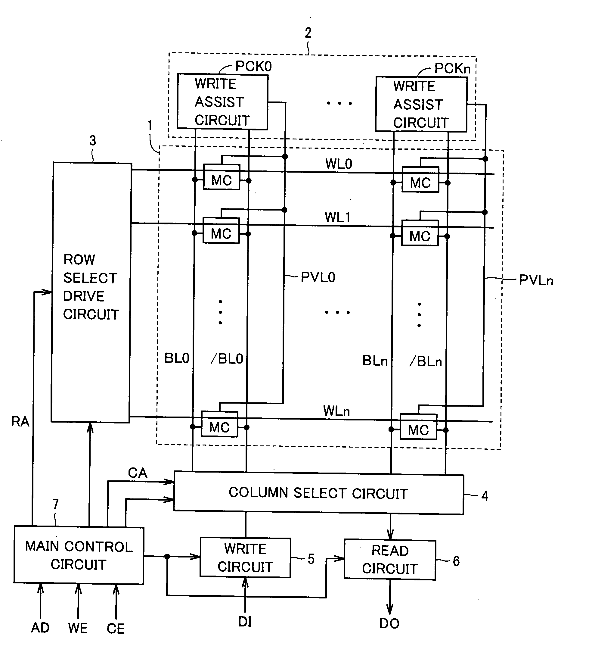
[0107]FIG. 4 shows a construction of the write assist circuit according to the first embodiment of the invention. FIG. 4 shows a construction of the write assist circuit provided for one bit line pair BL and / BL. In FIG. 4, memory cells MC in one column are connected to a common bit line pair BL and / BL. A high-side power supply line (which will be referred to as a “VDD source line” hereinafter) VDM transmitting high-side power supply voltage VDD is arranged as the cell power supply line for bit line pair BL and / BL. VDD source line VDM is connected to high-side power supply nodes VH of memory cells MC on the corresponding column.

[0108] The write assist circuits include write assist circuits PCKa and PCKb arranged at opposite ends of VDD source line VDM, respectively. Write assist circuits PCKa and PCKb have the same circuit construction, and corresponding portions are allotted with the same reference numerals.

[0109] Write assist circuit PCKa includes an inverter IV1 receiving a v...

second embodiment

[0141]FIG. 8 schematically shows a construction of a portion (memory cell circuit) related to memory cells MC in one row of a semiconductor memory device according to a second embodiment of the invention. In the construction shown in FIG. 8, write assist circuits PCKa and PCKb are arranged on the opposite sides of VDD source line VDM. VDD source line VDM is individually arranged for each column, and is commonly coupled to high-side power supply nodes VH of memory cells MC arranged in alignment in the corresponding column. In FIG. 8, memory cells MC arranged in four rows are shown as a representative example. Word lines WL0-WL3 are arranged corresponding to the respective memory cell rows.

[0142] Bit lines BL and / BL are arranged corresponding to the memory cell column, and bit lines BL and / BL are coupled to an internal data bus IO via column select gate CSG. Column select gate CSG is selectively made conductive to couple corresponding bit lines BL and / BL to internal data bus IO ac...

third embodiment

[0157]FIG. 10 schematically shows a construction of a memory cell array of the semiconductor memory device according to a third embodiment of the invention. FIG. 10 schematically shows a circuit construction for memory cells MC arranged in four rows and four columns. Bit line pairs BL0 and / BL0, BL1 and / BL1, BL2 and / BL2, and BL3 and / BL3 are arranged corresponding to the memory cell columns, respectively.

[0158] Bit lines BL0 and / BL0, and BL1 and / BL1 are coupled to a two-to-one selector 4b0, and bit lines BL2 and / BL2, and BL3 and / BL3 are likewise coupled to a two-to-one selector 4b1. These two-to-one selectors 4b0 and 4b1 perform two-to-one selection according to column address signal CA, and each selects one bit line pair from the corresponding two bit line pairs.

[0159] A write driver 5a0 and a sense amplifier circuit 6a0 are arranged for two-to-one selector 4b0, and a write driver 5a1 and a sense amplifier circuit 6a1 are arranged for two-to-one selector 4b1.

[0160] These t...


PUM


Abstract

Cell power supply lines are arranged for memory cell columns, and adjust impedances or voltage levels of the cell power supply lines according to the voltage levels of bit lines in the corresponding columns, respectively. In the data write operation, the cell power supply line is forced into a floating state according to the bit line potential on a selected column and has the voltage level changed, and a latching capability of a selected memory cell is reduced to write data fast. Even with a low power supply voltage, a static semiconductor memory device that can stably perform write and read of data is implemented.

Description

BACKGROUND OF THE INVENTION [0001] 1. Field of the Invention [0002] The present invention relates to a semiconductor memory device, and particularly to a static semiconductor memory device (Static Random Access Memory; SRAM) of which memory cells include inverter latches. More particularly, the invention relates to a configuration for stably writing and reading data even under a low power supply voltage condition in a static semiconductor memory device. [0003] 2. Description of the Background Art [0004] When transistors are miniaturized with development of miniaturization technology, voltage scaling according to the miniaturization is required from the viewpoint of reliability and power consumption. However, an influence by variations in manufacturing parameters increases in accordance with miniaturization, and accordingly, threshold voltages of transistors forming memory cells vary increasingly so that an operation margin of a memory lowers, and it becomes difficult to perform stab...

Claims


Application Information

Patent Timeline
Patent Type & Authority Applications(United States)
IPC IPC(8): G11C5/14
CPCG11C5/063G11C11/419G11C11/412
Inventor NII, KOJIOBAYASHI, SHIGEKIMAKINO, HIROSHIISHIBASHI, KOICHIROSHINOHARA, HIROFUMI
Owner RENESAS ELECTRONICS CORP
Why Eureka
Try Eureka