

Cascode circuit
a cascode circuit and circuit technology, applied in the field of cascode circuits, can solve the problems of increasing chip area, and unable to achieve satisfactory gain in cascode circuits
- Summary
- Abstract
- Description
- Claims
- Application Information
AI Technical Summary
Benefits of technology
Problems solved by technology
Method used
Image

Examples
embodiment 1
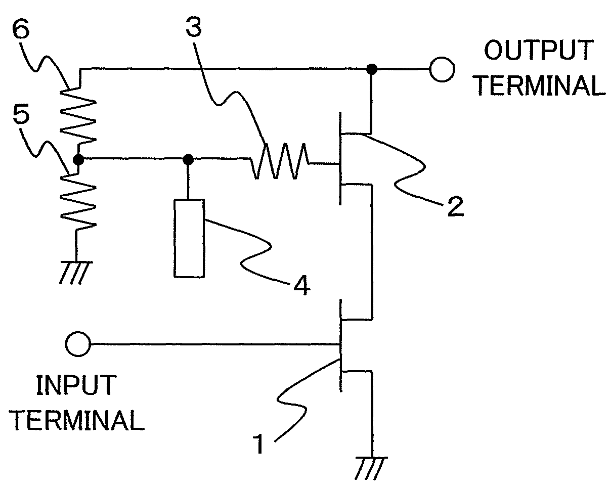
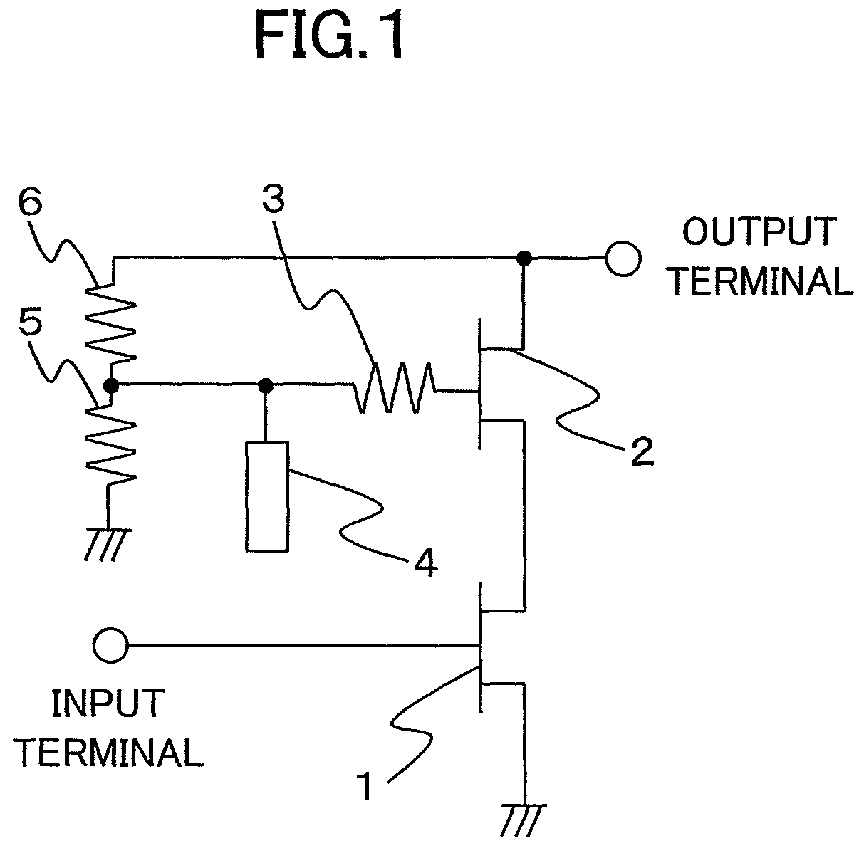
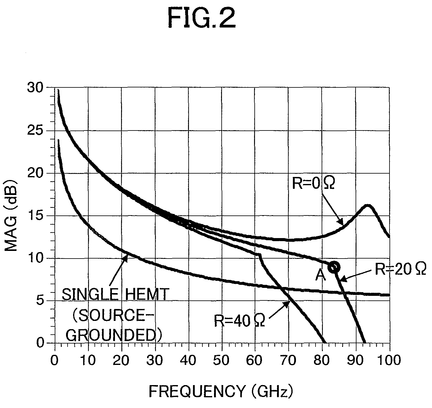
[0057]FIG. 1 is a circuit diagram illustrating a cascode circuit according to Embodiment 1 of the present invention. It is to be noted that the cascode circuit is formed such that its MAG is optimized at 76 GHz (predetermined frequency).
[0058]In FIG. 1, a drain of a source-grounded HEMT 1 (first transistor) is connected to a source of a gate-grounded HEMT 2 (second transistor). In other words, the HEMT 1 and the HEMT 2 are cascode-connected. A gate of the HEMT 1 is connected to an input terminal and a drain of the HEMT 2 is connected to an output terminal.
[0059]A gate of the HEMT 2 is connected to a reflection gain restricting resistance 3 (signal improving circuit) for restricting a reflection gain. An open stub 4 (filter circuit) for short-circuiting high-frequency signals in the predetermined frequency including the vicinity of the frequency is connected to a side of the reflection gain restricting resistance 3, which is opposite to the HEMT 2. Here, a length of the open stub 4 i...
embodiment 2
[0083]FIG. 6 is a circuit diagram illustrating an amplifier according to Embodiment 2 of the present invention. It is to be noted that the amplifier is formed such that its gain is the highest at 76 GHz (predetermined frequency).
[0084]In FIG. 6, an HEMT 1 and an HEMT 2 are cascode-connected. A gate of the HEMT 1 is connected to an input terminal and a drain of the HEMT 2 is connected to an output terminal.
[0085]A gate of the HEMT 2 is connected to a reflection gain restricting resistance 3 for restricting a reflection gain. Divider resistances 5 and 6 for setting a gate voltage of the HEMT 2 are connected between a source of the HEMT 1 and the gate of the HEMT 2 and between the gate and the drain of the HEMT 2, respectively.
[0086]Instead of the linear open stub 4 illustrated in FIG. 1, a fan-shaped radial stub 7 is connected to a side of the reflection gain restricting resistance 3, which is opposite to the HEMT 2. Similarly to the open stub 4, a length of the radial stub 7 is set s...
embodiment 3
[0097]FIG. 9 is a circuit diagram illustrating an amplifier according to Embodiment 3 of the present invention. It is to be noted that the amplifier is formed as a wideband amplifier which can be used over a wide band.
[0098]In FIG. 9, an HEMT 1 and an HEMT 2 are cascode-connected. A gate of the HEMT 1 is connected to an input terminal and a drain of the HEMT 2 is connected to an output terminal.
[0099]A gate of the HEMT 2 is connected to a reflection gain restricting resistance 3 for restricting a reflection gain. An open stub 4 for short-circuiting high-frequency signals in a predetermined frequency including the vicinity of the frequency is connected to a side of the reflection gain restricting resistance 3, which is opposite to the HEMT 2. Here, a length of the open stub 4 is set to be shorter than ¼ the wavelength (λ / 4) of a high-frequency signal at the predetermined frequency to be used (for example, 76 GHz).
[0100]Instead of the divider resistance 5 illustrated in FIG. 1, a firs...
PUM
 Abstract
Description
Claims
Application Information