Method for forming high-drain-voltage tolerance MOSFET transistor in a CMOS process flow with double well dose approach
a technology of mosfet transistor and process flow, which is applied in the direction of mos devices, transistors, electrical equipment, etc., can solve the problems of adding cost and complexity to the manufacturing process of integrated circuits
- Summary
- Abstract
- Description
- Claims
- Application Information
AI Technical Summary
Benefits of technology
Problems solved by technology
Method used
Image

Examples
Embodiment Construction
[0014]The making and using of the presently preferred embodiments are discussed in detail below. It should be appreciated, however, that the present invention provides many applicable inventive concepts that can be embodied in a wide variety of specific contexts. The specific embodiments discussed are merely illustrative of specific ways to make and use the invention, and do not limit the scope of the invention.
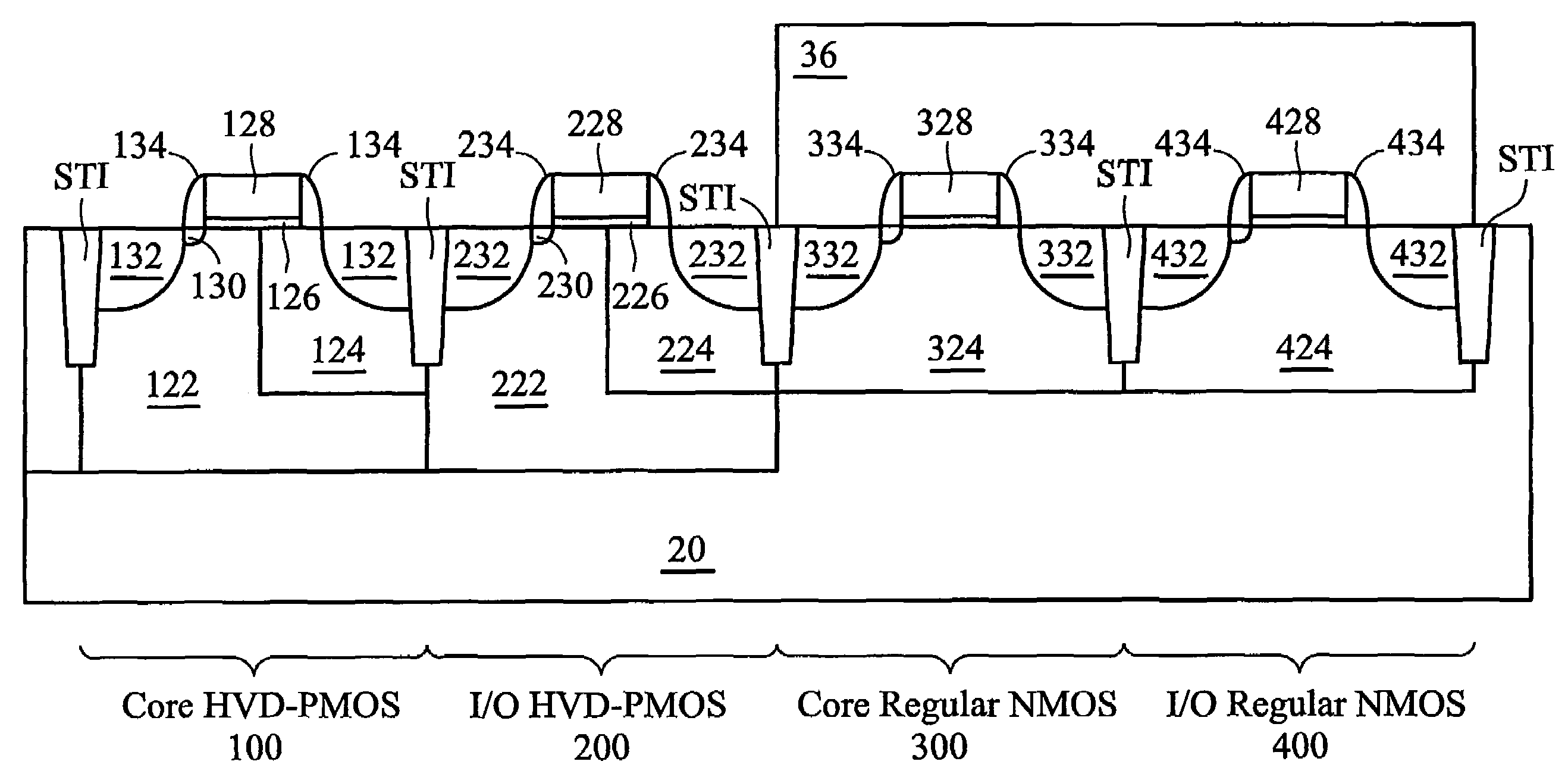
[0015]The intermediate stages of manufacturing the proposed high-voltage drain metal-oxide-semiconductor (HVD-MOS) devices are illustrated. The formation of p-type HVD-MOS (HVD-PMOS) devices is used as an example to explain the concept of the present invention. The variations of the preferred embodiments are then discussed. Throughout the various views and illustrative embodiments of the present invention, like reference numbers are used to designate like elements.
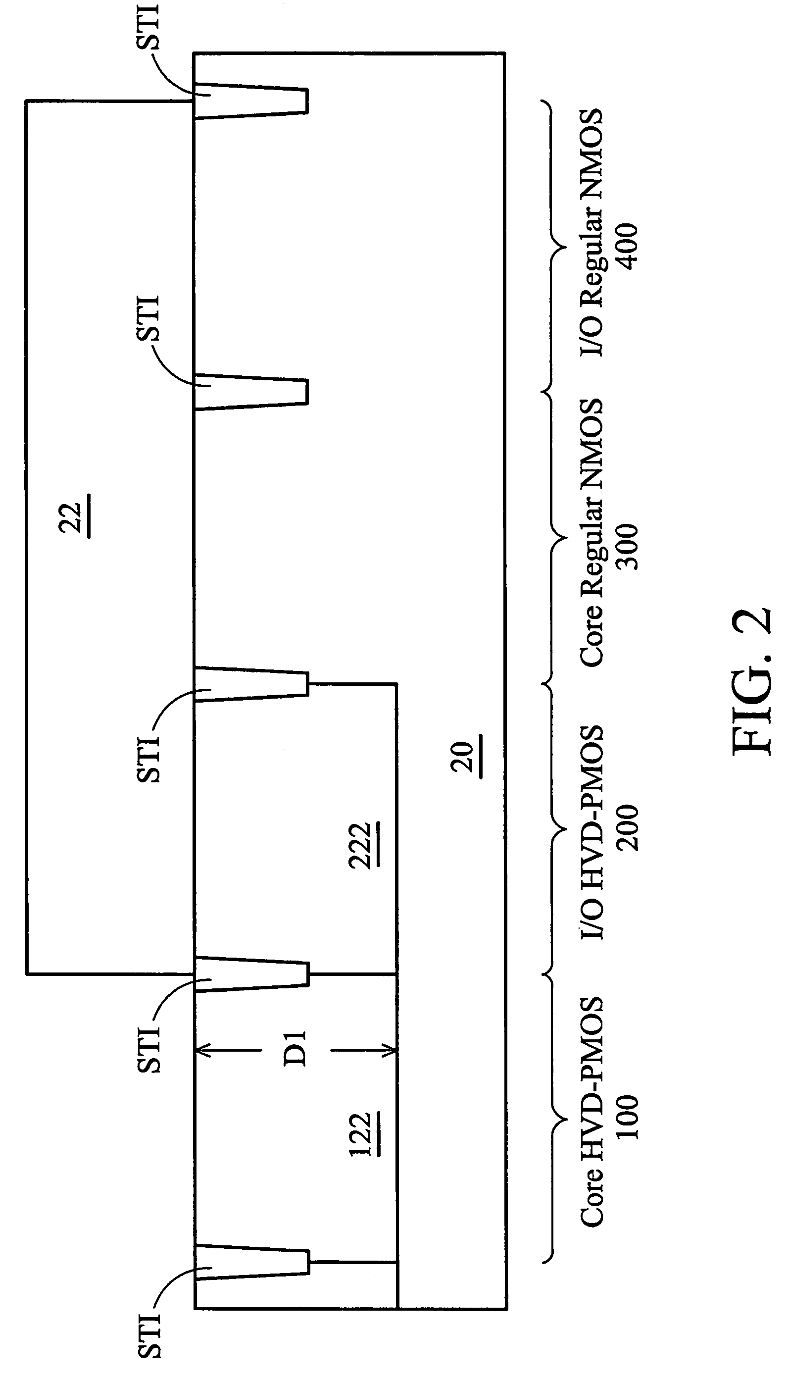
[0016]Referring to FIG. 2, a substrate 20 is provided. Substrate 20 is preferably formed of a semiconductor mater...
PUM
 Abstract
Description
Claims
Application Information