Method for joining adhesive tape to semiconductor wafer and method for separating protective tape from semiconductor wafer

a technology of adhesive tape and semiconductor wafer, which is applied in the manufacturing of semiconductor/solid-state devices, basic electric elements, electric devices, etc., can solve the problems of chip or crack, chip or crack deterioration, and high risk of damage to semiconductor wafers, so as to improve yield and less influence of defects

Inactive Publication Date: 2010-05-25
NITTO DENKO CORP
View PDF2 Cites 3 Cited by
  • Summary
  • Abstract
  • Description
  • Claims
  • Application Information

AI Technical Summary

Benefits of technology

[0007]A principal object of the present invention is to provide a method capable of suitably joining and separating an adhesive tape to and from a semiconductor wafer with less influence of a chip or a crack that occurs at an outer periphery of the semiconductor wafer.
[0012]By this method according to the present invention, a wafer that has been subjected to back grinding is attached to and held by a ring frame through an adhesive tape (a dicing tape) in order to prepare a mount frame. In this case, a joining direction (a joining roller moving direction) is determined diametrical from a position except a position of a defect. Thus, it is possible to reduce a stress applied to the wafer when the adhesive tape is joined to the wafer and to prevent further deterioration of the defect such as a chip or a crack.
[0020]By the method according to the present invention, a separating tape is joined to a protective tape joined to a front face of a wafer and, almost simultaneously, is separated and collected. Thus, the protective tape can be separated together with the separating tape from the front face of the wafer. In such separation, a tape separating direction is determined diametrical from a position except the defect position. Thus, it is possible to prevent the defect such as a chip or a crack from becoming further deteriorated due to a tape separating stress and a pressing force of a tape guide member each applied to the wafer.
[0024]As described above, the methods according to the present invention are effective at improving a yield in a process of manufacturing a semiconductor chip for the following reason that an adhesive tape can be joined to a semiconductor wafer or a protective tape can be separated from the semiconductor wafer with less influence of a defect such as a chip or a crack that occurs at an outer periphery of the semiconductor wafer.

Problems solved by technology

In a case where the semiconductor wafer is subjected to the processing of joining or separating such an adhesive tape, however, since a strength of the semiconductor wafer is insufficient due to its small thickness, there is a high risk of a damage of the semiconductor wafer due to a stress applied to the wafer when the adhesive tape is joined to / separated from the wafer.
In particular, a minute chip or crack occurs at an outer periphery of the wafer in the back grinding.
In such a case, there is a high possibility that the chip or the crack becomes deteriorated due to the stress applied to the wafer when the adhesive tape is joined to / separated from the wafer.

Method used


Image

  • Method for joining adhesive tape to semiconductor wafer and method for separating protective tape from semiconductor wafer
  • Method for joining adhesive tape to semiconductor wafer and method for separating protective tape from semiconductor wafer
  • Method for joining adhesive tape to semiconductor wafer and method for separating protective tape from semiconductor wafer

Examples


Embodiment Construction

[0034]Hereinafter, description will be given of one embodiment of the present invention with reference to the drawings.

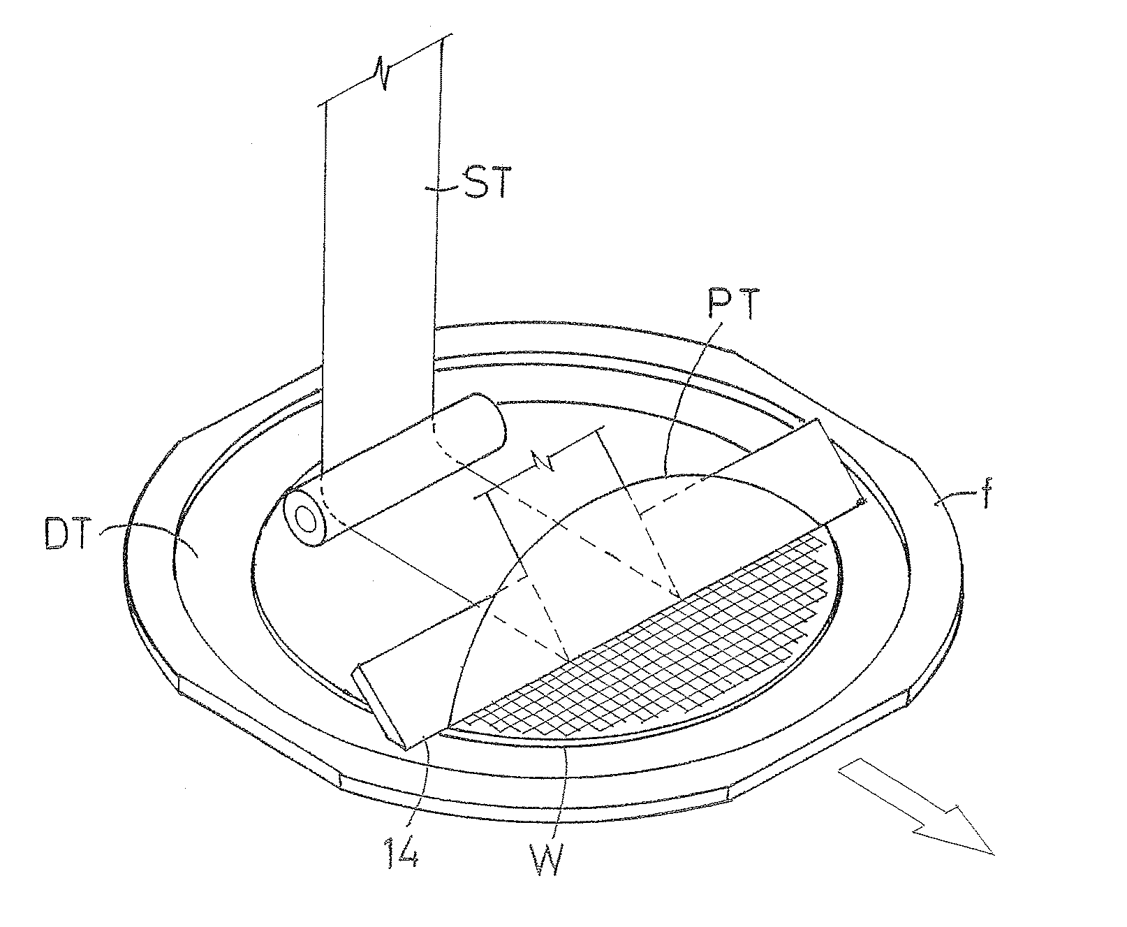
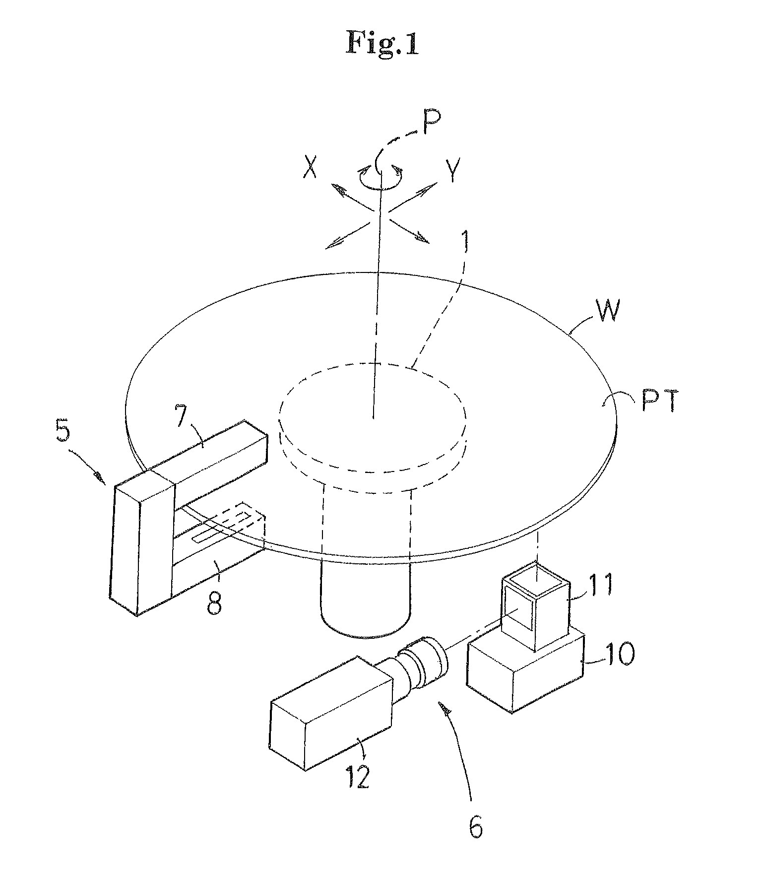
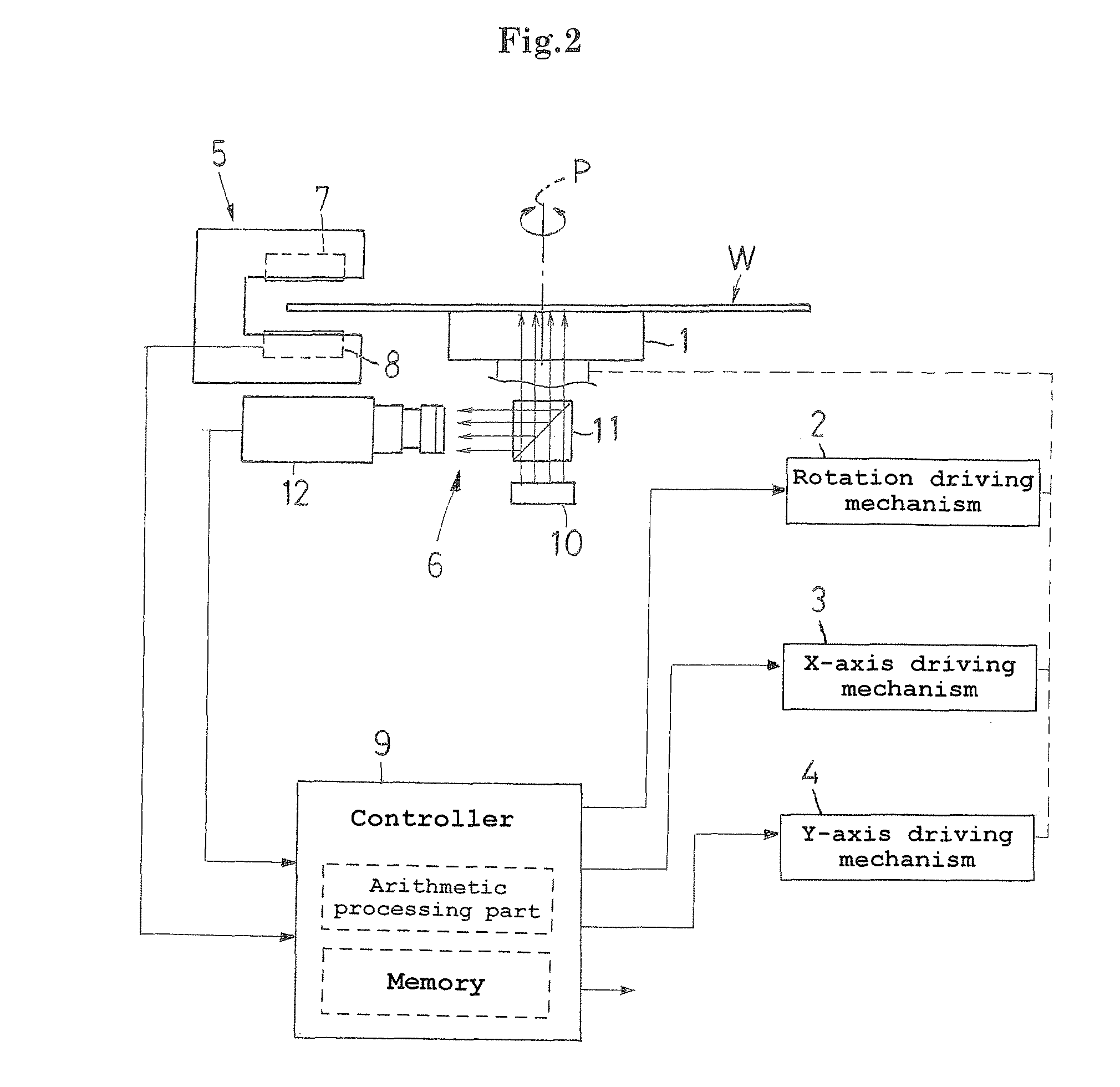
[0035]FIG. 1 is a perspective view showing main components of an aligner for use in alignment of a semiconductor wafer (hereinafter, simply referred to as a wafer) W. FIG. 2 shows a linkup in the aligner. FIG. 5 is a perspective view showing a back face of the wafer W to be subjected to processes. FIG. 6 is a sectional view partially showing the wafer W.

[0036]As shown in FIGS. 5 and 6, the wafer W has a front face on which a circuit pattern is formed, and a protective tape PT is joined to the front face. In this state, a back face of the wafer W is subjected to grinding, and then a metal layer M is deposited on the back face. Accordingly, the metal layer M is also deposited on the bared protective tape PT at a portion corresponding to a notch K formed as an alignment site at an outer periphery of the wafer W.

[0037]As shown in FIGS. 1 and 2, the aligner is rotatable ...


PUM


Abstract

An arithmetic processing part in a controller detects a position of a defect such as a chip or a crack that occurs at an outer periphery of a semiconductor wafer, and then a memory in the controller stores position information of the defect. The controller reads the position information of the defect through a network in each process. On the basis of this position information, the controller determines a direction of joining a dicing tape to the semiconductor wafer or a direction of separating a protective tape from a front face of the semiconductor wafer.

Description

BACKGROUND OF THE INVENTION[0001](1) Field of the Invention[0002]The present invention relates to a method for joining and separating an adhesive tape such as a protective tape to and from a pattern formation side of a semiconductor wafer.[0003](2) Description of the Related Art[0004]A chip component is fabricated from a semiconductor wafer (hereinafter, appropriately referred to as a “wafer”) in the following manner. For example, a circuit pattern is formed on a front face of a wafer, and then a protective tape is joined to the front face of the wafer. Thereafter, a back face of the wafer is subjected to a grinding process (back grinding) such that the wafer has a small thickness. The wafer having the small thickness is attached to and held by a ring frame through a dicing tape. Thereafter, the protective tape is separated from the front face of the wafer, and then the wafer is transported to a dicing process (refer to, for example, JP-A 2002-124494).[0005]As described above, the p...

Claims


Application Information

Patent Timeline
Patent Type & Authority Patents(United States)
IPC IPC(8): H01L21/00
CPCH01L21/67288H01L21/67132H01L21/68H01L21/30H01L21/02
Inventor YAMAMOTO, MASAYUKIIKEDA, SATOSHI
Owner NITTO DENKO CORP
Why Eureka
Try Eureka