Semiconductor device and display device utilizing the same

a semiconductor device and display device technology, applied in the direction of static storage, digital storage, instruments, etc., can solve the problems of easy variation of electric characteristics and inability to distinguish sources and drains, and achieve the effects of small influence of characteristics of adjacent transistors, less influence of minute current, and large current in output operation

Inactive Publication Date: 2008-03-18
SEMICON ENERGY LAB CO LTD
View PDF31 Cites 39 Cited by
  • Summary
  • Abstract
  • Description
  • Claims
  • Application Information

AI Technical Summary

Benefits of technology

[0072]According to the invention, a source-drain voltage of one of two transistors connected in series becomes extremely small in the set operation, thus the set operation is performed to the other transistor. Then, in the output operation, the two transistors operate as a multi-gate transistor, therefore, a current value in the output operation can be small. In other words, a current in the set operation can be large. Therefore, the set operation can be performed rapidly without being influenced by an intersection capacitance and a wiring resistance which are parasitic on a wiring and the like.
[0073]As the current in the output operation can be large, there is less influence of a minute current due to noise and the like.
[0074]Furthermore, a common transistor is used in a part of the set operation and the output operation, therefore, an influence of variations in characteristics of adjacent transistors can be small.

Problems solved by technology

A TFT includes three terminals: a gate, a source, and a drain, however, the source and drain cannot be distinguished because of the structure of TFT.
On the other hand, its electric characteristics tend to vary easily due to a defect in the crystal grain boundary.

Method used


Image

  • Semiconductor device and display device utilizing the same
  • Semiconductor device and display device utilizing the same
  • Semiconductor device and display device utilizing the same

Examples


embodiment mode 1

[0127]The invention can be applied not only to a pixel having an EL element but also to various analog circuits having a power supply. In this embodiment mode, the basic principle of the invention is described.

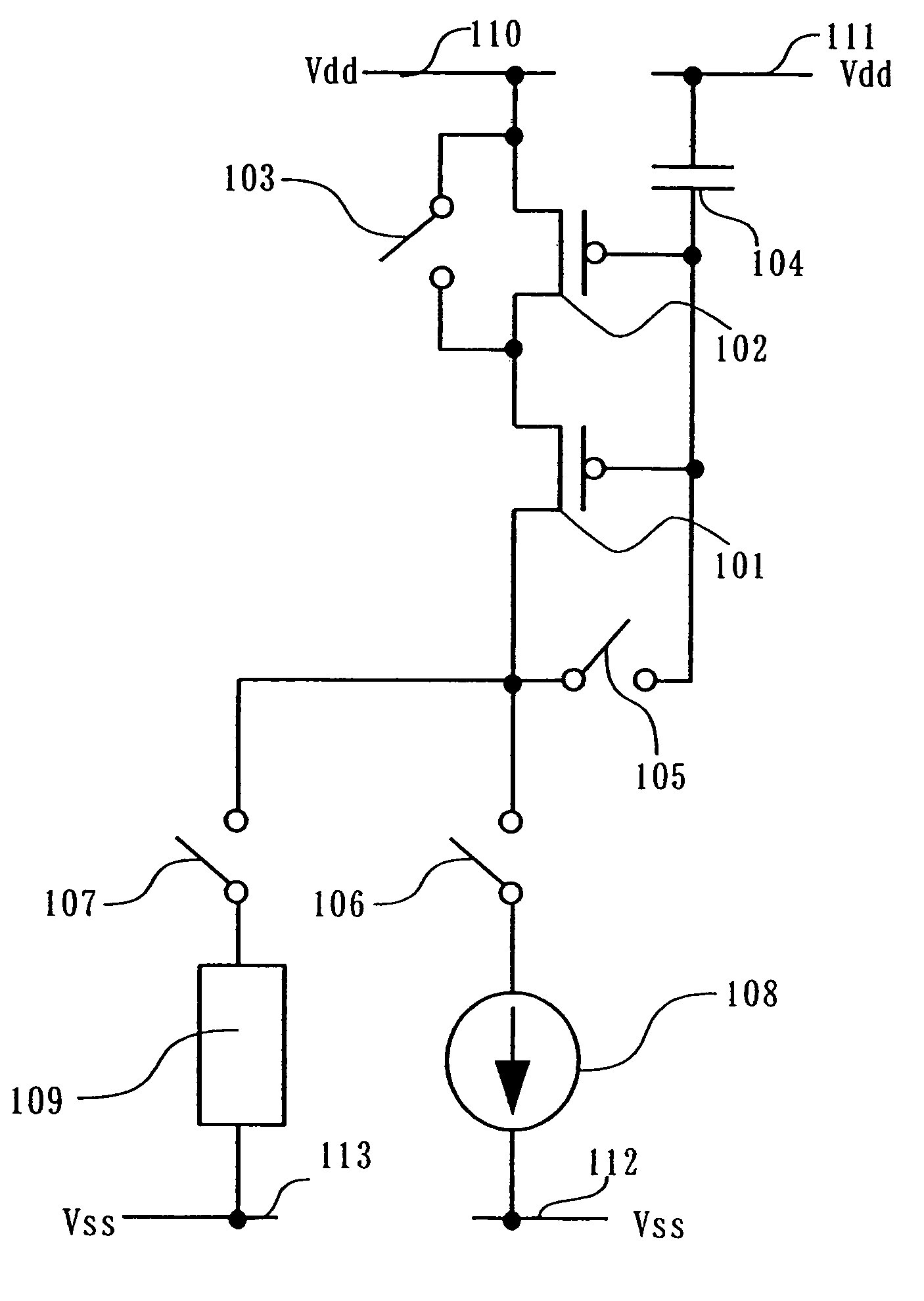
[0128]First, FIG. 1 shows a configuration based on the basic principle of the invention. A current source transistor 101 which constantly operates as a current source (or a part of it) and a switching transistor 102 of which operation changes according to the circumstance are provided, and the current source transistor 101, the switching transistor 102, and a wiring 110 are connected in series.

[0129]A gate terminal of the current source transistor 101 is connected to one terminal of a capacitor 104. The other terminal of the capacitor 104 is connected to a wiring 111. Therefore, it is possible to hold a potential of the gate terminal of the current source transistor 101.

[0130]Further, the gate terminal and a drain terminal of the current source transistor 101 are connected to ...

embodiment mode 2

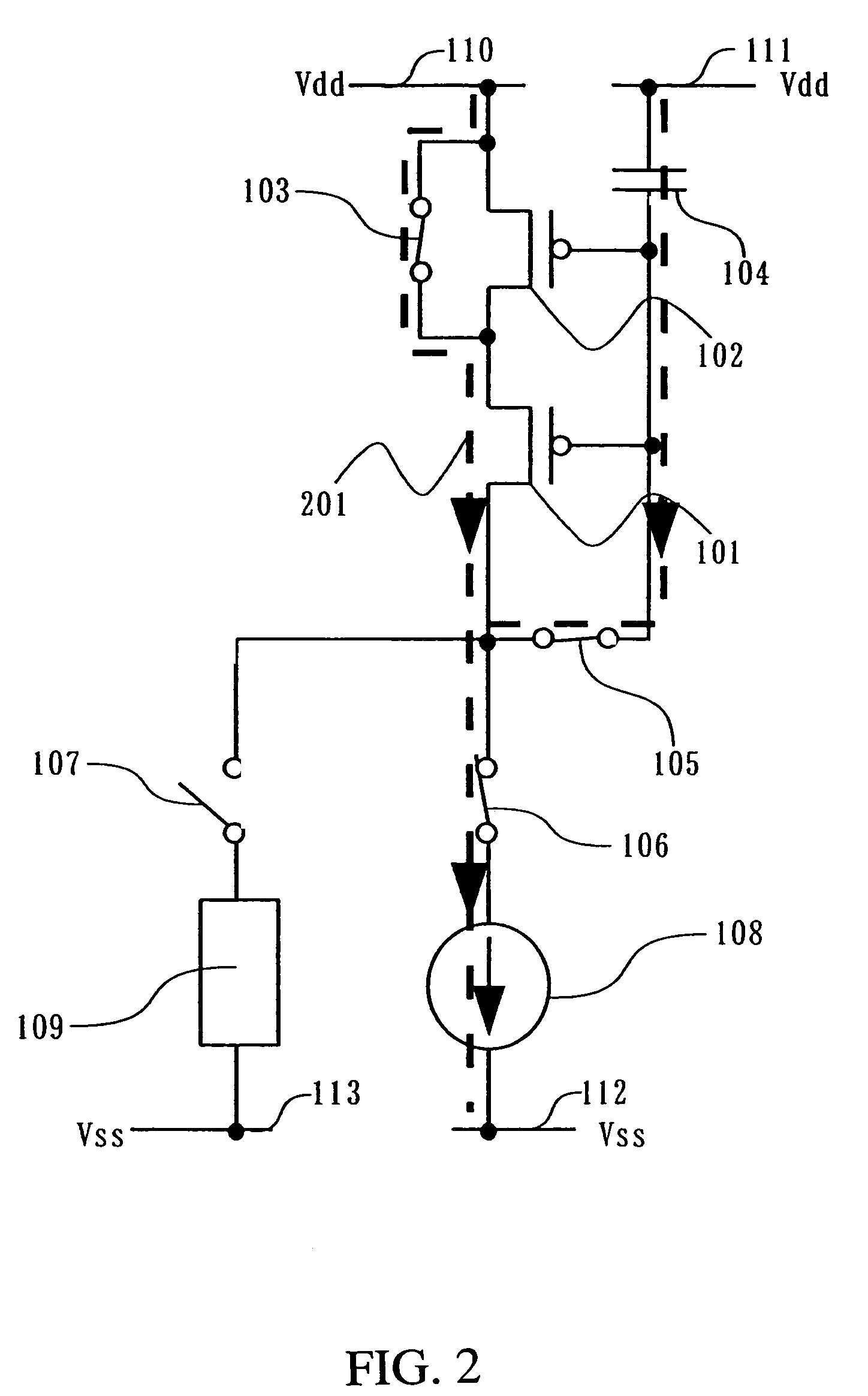
[0167]In Embodiment Mode 1, the configuration of FIG. 1 is employed for realizing the current source operation and the short-circuit operation respectively to the switching transistor 102. In this embodiment mode, an example of a configuration for realizing the current source operation and the short-circuit operation, which is different from Embodiment Mode 1 is shown.

[0168]It should be noted that most of the description which is similar to Embodiment Mode 1 will be omitted here.

[0169]First, FIG. 26 shows a second configuration in which the current source operation and the short-circuit operation are realized respectively to the switching transistor 102.

[0170]In FIG. 1, the switch 103 is used so that the switching transistor 102 can perform the short-circuit operation. By controlling the switch 103, a current does not flow between the source and drain of the switching transistor 102 so the source terminal and the drain terminal of the switching transistor 102 have approximately the ...

embodiment mode 3

[0187]Described in this embodiment mode is the case where the circuits described in Embodiment Modes 1 and 2 are changed partially.

[0188]The case where the circuit of FIG. 1 is changed partially is described here for simplicity. Therefore, most of the description which is similar to Embodiment Mode 1 will be omitted here. However, it can be applied to various circuits described in Embodiment Modes 1 and 2.

[0189]First, FIG. 36 shows FIG. 1 of which configuration is changed partially. FIG. 36 is different from FIG. 1 in the respect that the switch 107 in FIG. 1 is changed to a multi transistor 3601. The multi transistor 3601 is a transistor having the same polarity (conductivity) as the current source transistor 101 and the switching transistor 102. A gate terminal of the multi transistor 3601 is connected to a gate terminal of the current source transistor 101. The multi transistor 3601 changes its operation according to the circumstance. That is, it operates as a switch in the set o...


PUM


Abstract

A source-drain voltage of one of two transistors connected in series becomes quite small in a set operation (write signal), thus the set operation is performed to the other transistor. In an output operation, two transistors operate as a multi-gate transistor, therefore, a current value can be small in the output operation. In other words, a current can be large in the set operation. Therefore, the set operation can be performed rapidly without being easily influenced by an intersection capacitance and a wiring resistance which are parasitic on a wiring and the like. Further, an influence of variations between adjacent ones can be small as one same transistor is used in the set operation and the output operation.

Description

TECHNICAL FIELD[0001]The present invention relates to a structure of a semiconductor device. More particularly, the invention relates to a structure of an active matrix semiconductor device including a thin film transistor (hereinafter referred to as a TFT) formed on an insulator such as a glass and plastic.BACKGROUND ART[0002]In recent years, a self-luminous type display device such as an electro luminescence (EL) display device and an FED (Field Emission Display) has been actively developed. A self-luminous display device is advantageous since it is highly visible, suitable for thin design as it does not require a backlight required in a liquid crystal display device (LCD) and the like, and its viewing angle is almost unlimited.[0003]An EL element denotes an element having a light emitting layer in which a luminescence is obtained by applying electric field. The light emitting layer emits light when returning from a singlet excited state to a base state (fluorescence) and when ret...

Claims


Application Information

Patent Timeline
Patent Type & Authority Patents(United States)
IPC IPC(8): G09G3/30
CPCG09G3/325G09G3/3283G09G2300/0828G09G2320/0223G09G2300/0861G09G2310/0251G09G2300/0842G09G3/30G09G2300/0814
Inventor KIMURA, HAJIME
Owner SEMICON ENERGY LAB CO LTD
Why Eureka
Try Eureka