Compound semiconductor epitaxial substrate and method for manufacturing the same
a semiconductor and epitaxial substrate technology, applied in the direction of basic electric elements, electrical apparatus, semiconductor devices, etc., can solve the problems of ingaas constant increasing, mbe method being inferior in mass-productivity, and lattice misfitting with the electron supply layer or the substrate material
- Summary
- Abstract
- Description
- Claims
- Application Information
AI Technical Summary
Problems solved by technology
Method used
Image

Examples
example 1
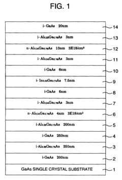
[0044]An epitaxial substrate having a layer structure shown in FIG. 1 was fabricated as described below by the use of a low pressure barrel-typed MOCVD reactor.
[0045]A semi-insulating GaAs single crystal substrate manufactured by the VGF method was prepared as a GaAs single crystal substrate 1, and respective compound semiconductor layers were epitaxially grown on the GaAs single crystal substrate 1. Trimethyl gallium (TMG), trimethyl aluminum (TMA), and trimethyl indium (TMI) were used as source materials of the third-group elements, while arsine (AsH3) was used as a source material of the fifth-group element. Silicon (Si) was used as an n-type dopant. High-purity hydrogen was used as a carrier gas for the source materials, and the epitaxial growth was performed under the conditions that a pressure within the reactor was 0.1 atm, a growth temperature was 650° C., and a growth rate was 3 to 1 μM / hr.
[0046]The channel layer 9 through which electrons run was epitaxially grown in order ...
example 2
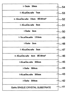
[0049]An epitaxial substrate having a layer structure shown in FIG. 3 was fabricated in accordance with the MOCVD method as in the case of Example 1. In the epitaxial substrate shown in FIG. 3, a reference numeral 21 denotes a semi-insulating GaAs single crystal substrate, reference numerals 22 to 25 denote buffer layers, a reference numeral 26 denotes a back side electron supplying layer, reference numerals 27 and 28 denote back side spacer layers, a reference numeral 29 denotes a channel layer, reference numerals 30 and 31 denote front side spacer layers, a reference numeral 32 denotes a front side electron supplying layer, a reference numeral 33 denotes an undoped AlGaAs layer, and a reference numeral 34 denotes an undoped GaAs layer. Composition and thickness of each layer are as shown in FIG. 3.
[0050]As can be seen from comparing FIG. 3 with FIG. 1, Example 2 is different from Example 1 in that a strain InGaAs layer having an In composition of 0.35 and a thickness of 5.5 nm is ...
PUM
 Abstract
Description
Claims
Application Information