Methods that involve electrodes, such as DC arc plasmas, can have disadvantages due to
electrode erosion and incorporation of material into the diamond.
Combustion methods avoid the
electrode erosion problem but are reliant on relatively expensive feed gases that must be purified to levels consistent with high quality diamond growth.
Also the temperature of the
flame, even when combusting oxy-
acetylene mixes, is insufficient to achieve a substantial fraction of atomic
hydrogen in the gas
stream and the methods rely on concentrating the flux of gas in a localized area to achieve reasonable growth rates.
Perhaps the principal reason why
combustion is not widely used for bulk diamond growth is the cost in terms of kWh of energy that can be extracted.
Hot filament reactors while appearing superficially simple have the
disadvantage of being restricted to use at lower gas pressures which are required to ensure relatively effective transport of their limited quantities of atomic
hydrogen to a growth surface.
One problem with fabricating polycrystalline CVD diamond optical components is that during the CVD growth process defects and / or impurities such as
nitrogen,
silicon and non-diamond carbon are incorporated into the diamond material as discussed below.
While
nitrogen is advantageous for achieving commercially useful growth rates, incorporation of
nitrogen into the
synthetic diamond material can detrimentally affect the optical and thermal performance characteristics of the material.
Silicon defects and / or impurities may come from
silicon based components within the CVD reactor.
Such
silicon containing
quartz components are exposed to extreme temperatures from the
plasma in use and this can result in silicon from these components being incorporated into the
synthetic diamond material.
However, this selective
etching process does not usually remove all the deposited non-diamond carbon and such material therefore becomes incorporated into the CVD diamond material forming defects.
Uniformity is an issue in terms of spatial variations in the rate of
impurity uptake across a growth surface and temporal variations in the rate of
impurity uptake over a growth run.
An increase in the size of grains and grain boundaries as the synthetic
polycrystalline diamond wafer grows thicker leads to an increase in the rate of defect and / or impurity uptake within the enlarged grain boundaries which can result in an increasing concentration of defects and / or defects and / or impurities through the thickness of a synthetic polycrystalline diamond wafer.
In addition to the above described problems, variations in growth rate across a synthetic polycrystalline diamond wafer can lead to variations in impurity uptake.
Furthermore, variations in growth rate also cause variations in thickness which can lead to strain and
cracking of synthetic polycrystalline diamond wafer on cooling after completion of the CVD growth process.
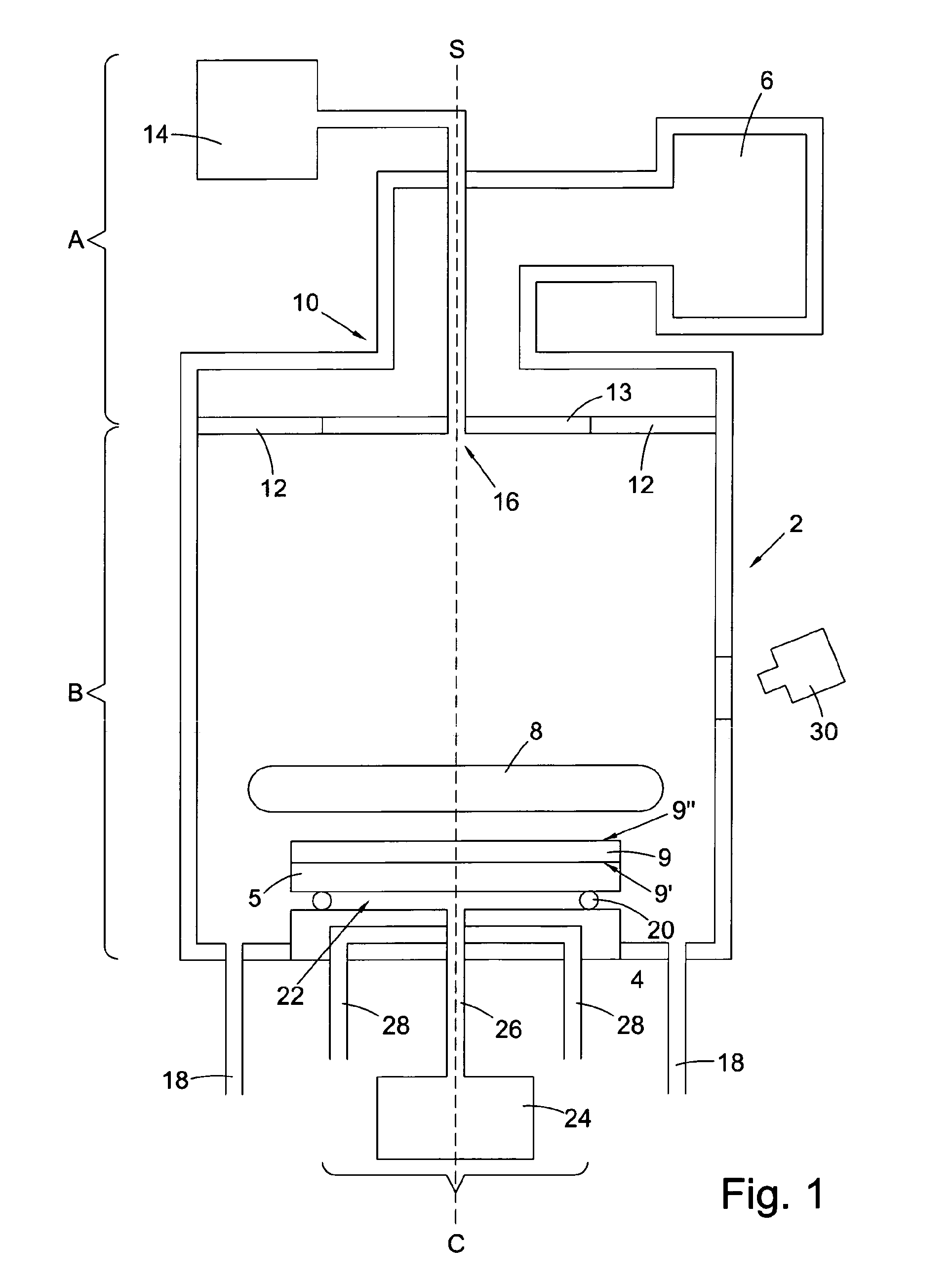
Variations in growth rate can be caused by non-uniformities in the
plasma across the growth surface and non-uniformities in the temperature of the substrate on which the synthetic polycrystalline diamond wafer is grown.
However, the production of larger and / or thicker polycrystalline diamond wafers of high
optical quality has proved problematic.
While it has been possible to fabricate larger and / or thicker polycrystalline diamond wafers, these have been of lower
optical quality, particularly towards the periphery of the wafers.
Such wafers do not meet the requirements for certain commercial applications which require relatively thick, relatively large
diameter synthetic polycrystalline diamond windows of extremely high optical quality.
However these sizes and thicknesses are not high enough for certain applications.


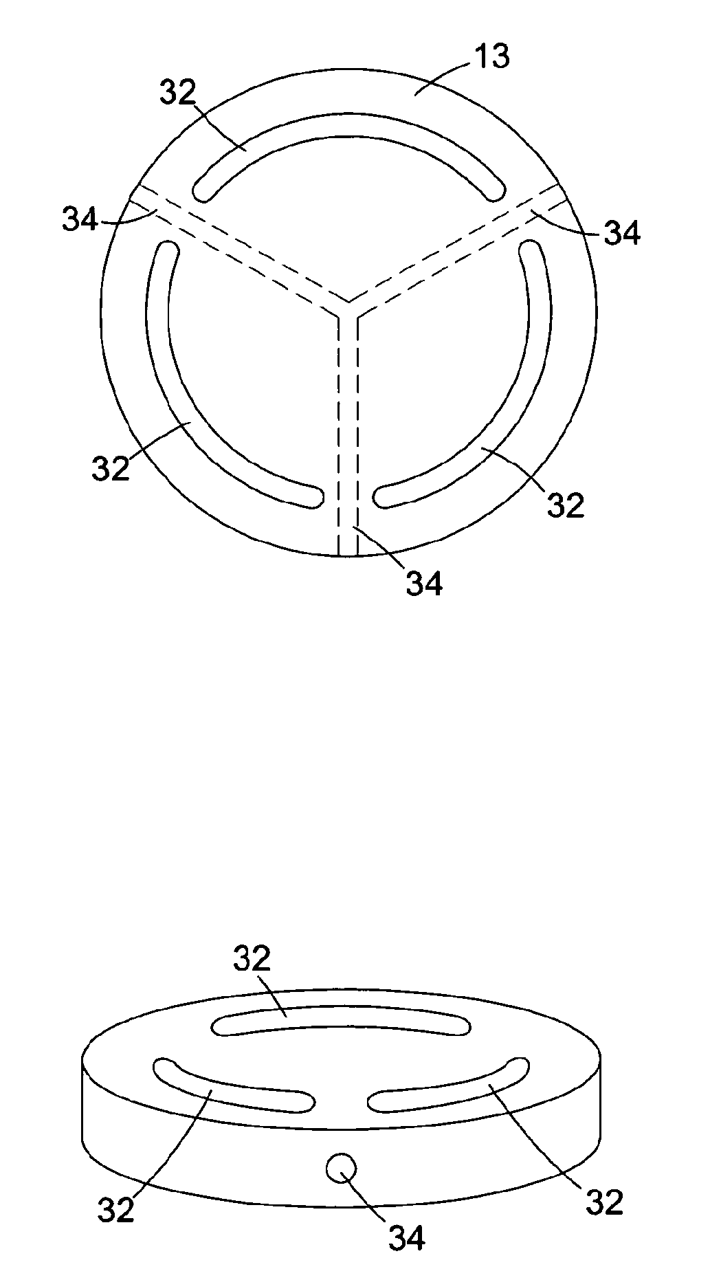
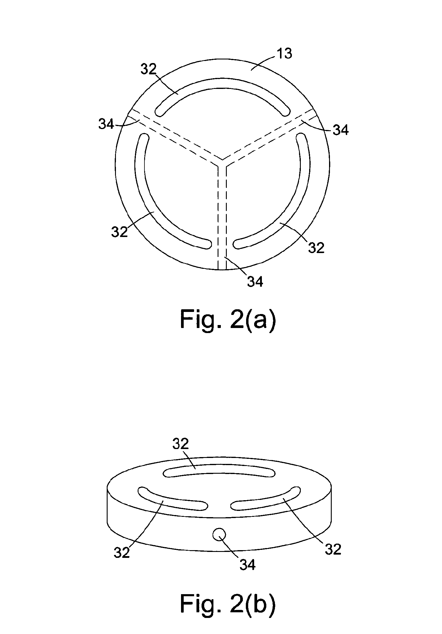