Transparent conductive articles and methods of making same

a transparent and conductive material technology, applied in the field of transparent substrates, can solve the problems of low resistivity, low oxygen and water vapor permeability of the layer, and low enough resistivity to function as an electrode for the display, etc., to achieve improved ruggedness, space-saving, and more portable

Inactive Publication Date: 2007-10-02
3M INNOVATIVE PROPERTIES CO
View PDF131 Cites 51 Cited by
  • Summary
  • Abstract
  • Description
  • Claims
  • Application Information

AI Technical Summary

Benefits of technology

[0005]The present invention is directed to the fabrication of flat panel displays on lightweight, flexible, plastic substrates. Because plastic substrates for FPDs are flexible, smaller and lighter than glass substrates, the electronic device with the plastic FPD is more portable, space-efficient and lightweight. In addition, electroluminescent and organic light emitting devices fabricated on flexible polymeric substrates in a coating process have lower manufacturing costs than those with glass substrates, and improved ruggedness.
[0007]Using a smoothing base coat layer over the plastic substrate imparts good optical quality throughout the substrate layers and provides a pristine surface for nucleation of the deposited barrier or conductive layer, e.g. TCO. The pristine surface smoothes over any surface roughness of the plastic substrate, thereby adding to the FPD lifetime and optical quality. Additionally, a hardcoat layer is applied over the substrate in lieu of or in addition to the smoothing basecoat layer.
[0010]The PML deposited organic polymer layer is used to produce substrate surface smoothing and improve barrier coatings in the multilayer structure. The benefit of a smooth substrate surface is that there is a clean surface for adhesion, nucleation, and growth of a deposited conductive layer, e.g. a TCO. Additionally, a PML deposited organic polymer layer provides protection of an underlying barrier layer in order to minimize holes or other defects in the layer so that there is low permeability.
[0012]In an embodiment, a PML processed top coat polymer layer is applied before the previously deposited layer contacts a surface, such as a roller, thereby protecting the previously deposited layer. The PML processed top coat greatly enhances the exclusion of moisture (water vapor) and atmospheric gases that chemically degrade the display medium and decrease the device performance, even though the polymer topcoat is not, itself, a good barrier material.
[0015]The thin layers of TCO are preferably separated by layers deposited using the PML process, which leads to improved optical, electrical and mechanical performance. Superior surface properties (low surface roughness, and high optical quality), barrier properties (low vapor permeability) and mechanical properties result when TCO coatings are deposited by magnetron sputtering on a plastic substrate in combination with the PML process, e.g., by providing hydrogen in the plasma of the vacuum chamber used in the sputtering process of the TCO. Preferably, moderate annealing temperature conditions are used for TCO deposition. For example, the resistivity of ITO is a function of the oxygen and tin content, as well as the deposition conditions (e.g., temperature). Low temperature depositions yield high resistivity ITO layers. A low resistivity for the ITO layers is desired. The resistivity of ITO decreases with a thicker TCO layer. But as discussed previously, thick TCO layers are prone to cracking or crazing. Multiple thin layers of TCO, as described in the present invention, will not crack and will yield a lower resistivity. Moreover, the surface resistivity of a thin film of TCO in multiple layers is low for a given total film thickness, due to its improved microstructure.

Problems solved by technology

In particular, the layer has both low oxygen and water vapor permeability, and a low enough resistivity to function as an electrode for the display.

Method used


Image

  • Transparent conductive articles and methods of making same
  • Transparent conductive articles and methods of making same
  • Transparent conductive articles and methods of making same

Examples


Embodiment Construction

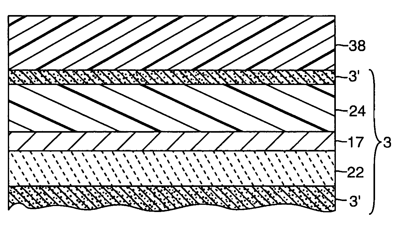
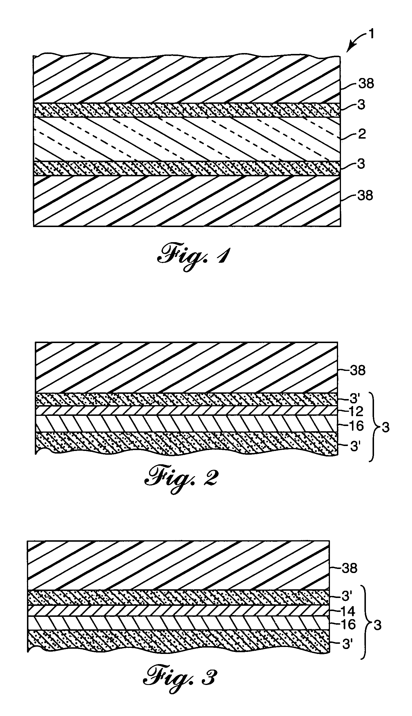
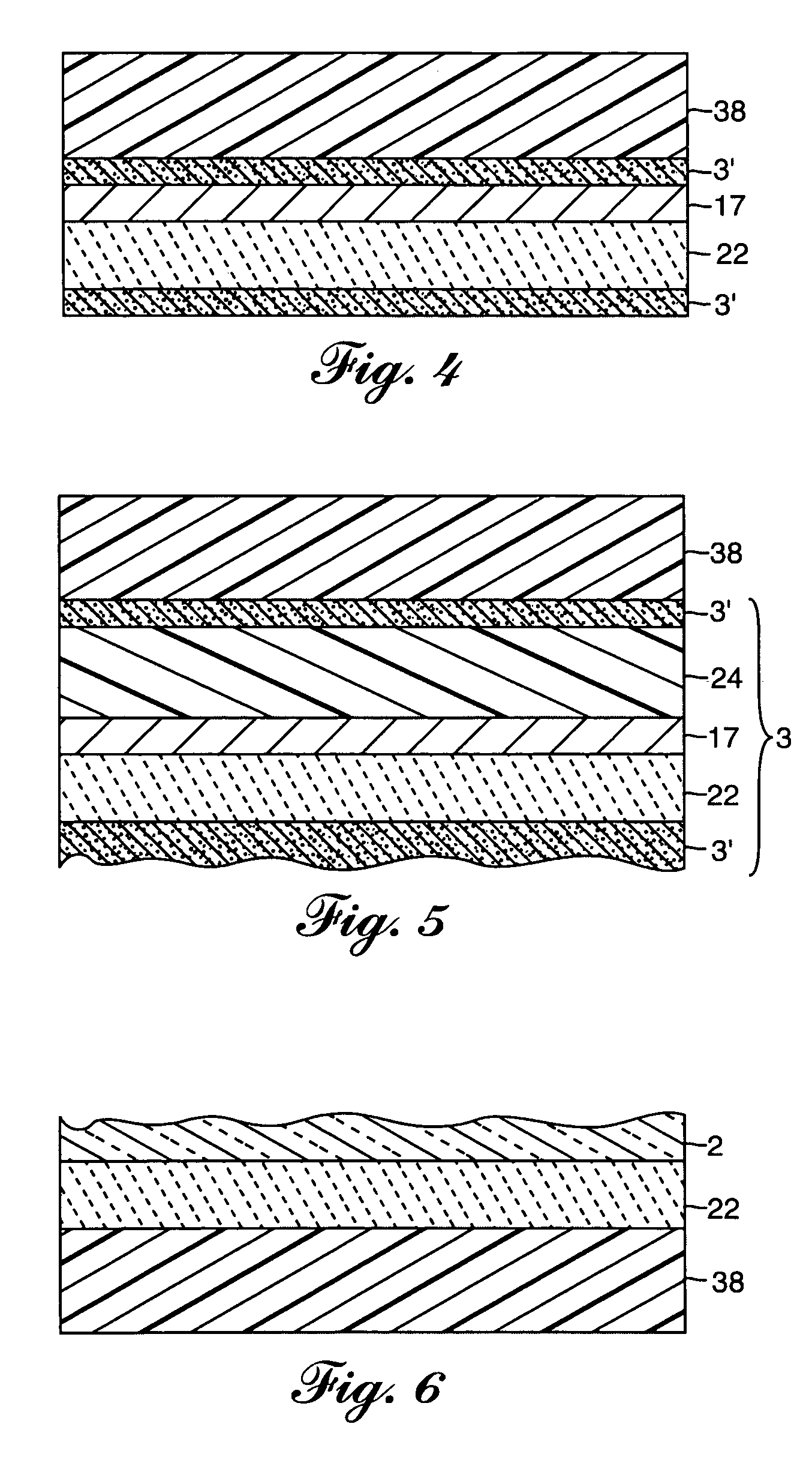
[0052]A flat panel display (FPD)1, of the present invention as shown in FIG. 1, employs lightweight, flexible, plastic substrates 38 for constructing FPDs. In between two plastic substrates 38 of the flat panel display are at least two electrodes 3. At least one of the electrodes is transparent for viewing of a display medium 2 positioned between the two electrodes 3. The display medium, as well as some electrode material, are protected from oxidative degradation and reaction with or incorporation of moisture.

[0053]The displays are fabricated using plastic substrates such as various polyolefins, e.g. polypropylene (PP), various polyesters, e.g. PET and other polymers such as polyethylene naphthalate (PEN), polyethersulphone (PES), polyestercarbonate (PC), polyetherimide (PEI), polyarylate (PAR), polyimide (PI), and polymers with trade names ARTON™ (Japanese Synthetic Rubber Co., Tokyo, Japan) and AVATREL™ (B.F. Goodrich, Brecksville, Ohio). FIG. 37 shows deposition temperature capab...


PUM

PropertyMeasurementUnit
thicknessaaaaaaaaaa
sheet resistanceaaaaaaaaaa
optical densityaaaaaaaaaa

Abstract

An electronic device on a plastic substrate, at least one side of the device being protected from reaction with or incorporation of moisture by a composite barrier. The composite barrier may contain, for example, multiple layers of transparent conductive oxide separated by one or more vacuum-evaporated in-situ polymerized organic layers, or may contain multiple barrier layers of transparent conductive oxide, transparent metal, or transparent conductive metal nitride, separated by at least one layer of organic dielectric polymer.

Description

CROSS-REFERENCE TO RELATED APPLICATIONS[0001]This application claims the benefit of U.S. patent application Ser. No. 09 / 939,008, filed Aug. 24, 2001, which is a divisional of U.S. patent application Ser. No. 09 / 419,870 filed Oct. 18, 1999, now abandoned, which in turn claims the benefit of U.S. Provisional Application No. 60 / 106,871, filed Nov. 2, 1998, all of which are incorporated by reference, including the original specification, first substitute specification, second substitute specification, and all attached Appendices of U.S. patent application Ser. No. 09 / 419,870FIELD OF THE INVENTION[0002]This invention relates to composite substrates for flat panel displays (FPDs), packaging materials and light sources (electro luminescence lamps) comprising a plastic substrate having thin film barrier and conductive layers, in particular, multiple thin alternating layers of metallic film, transparent conductive oxide (TCO), metal nitride, and organic polymers deposited over the plastic su...

Claims


Application Information

Patent Timeline
Patent Type & Authority Patents(United States)
IPC IPC(8): B32B15/08G02F1/1333H01L51/52
CPCC23C16/0272C23C16/545G02F1/133345H01L51/5256H01L51/0097H01L51/5206G02F1/133305Y10T428/12576H01L2251/5338Y02E10/549Y10T428/31681Y10T428/31794Y10T428/31678Y10T428/31667Y10T428/31692Y10T428/31935Y02P70/50H10K77/111H10K50/81H10K50/816H10K50/8445H10K2102/311
Inventor BRIGHT, CLARK I.
Owner 3M INNOVATIVE PROPERTIES CO
Why Eureka
Try Eureka