Emulation system with time-multiplexed interconnect

Inactive Publication Date: 2010-06-15
CADENCE DESIGN SYST INC
View PDF28 Cites 26 Cited by
  • Summary
  • Abstract
  • Description
  • Claims
  • Application Information

AI Technical Summary

Benefits of technology

[0014]A new type of hardware emulation system is disclosed and claimed which reduces hardware cost by time-multiplexing multiple design signals onto physical logic chip pins and printed circuit board traces but which does not have the limitations of low operating

Problems solved by technology

A new type of hardware emulation system is disclosed and claimed which reduces hardware cost by time-multiplexing multiple design signals onto physic

Method used


Image

  • Emulation system with time-multiplexed interconnect
  • Emulation system with time-multiplexed interconnect
  • Emulation system with time-multiplexed interconnect

Examples


Example

DETAILED DESCRIPTION OF THE DRAWINGS

[0065]Turning to the figures, the presently preferred apparatus and methods of the present invention will now be described.

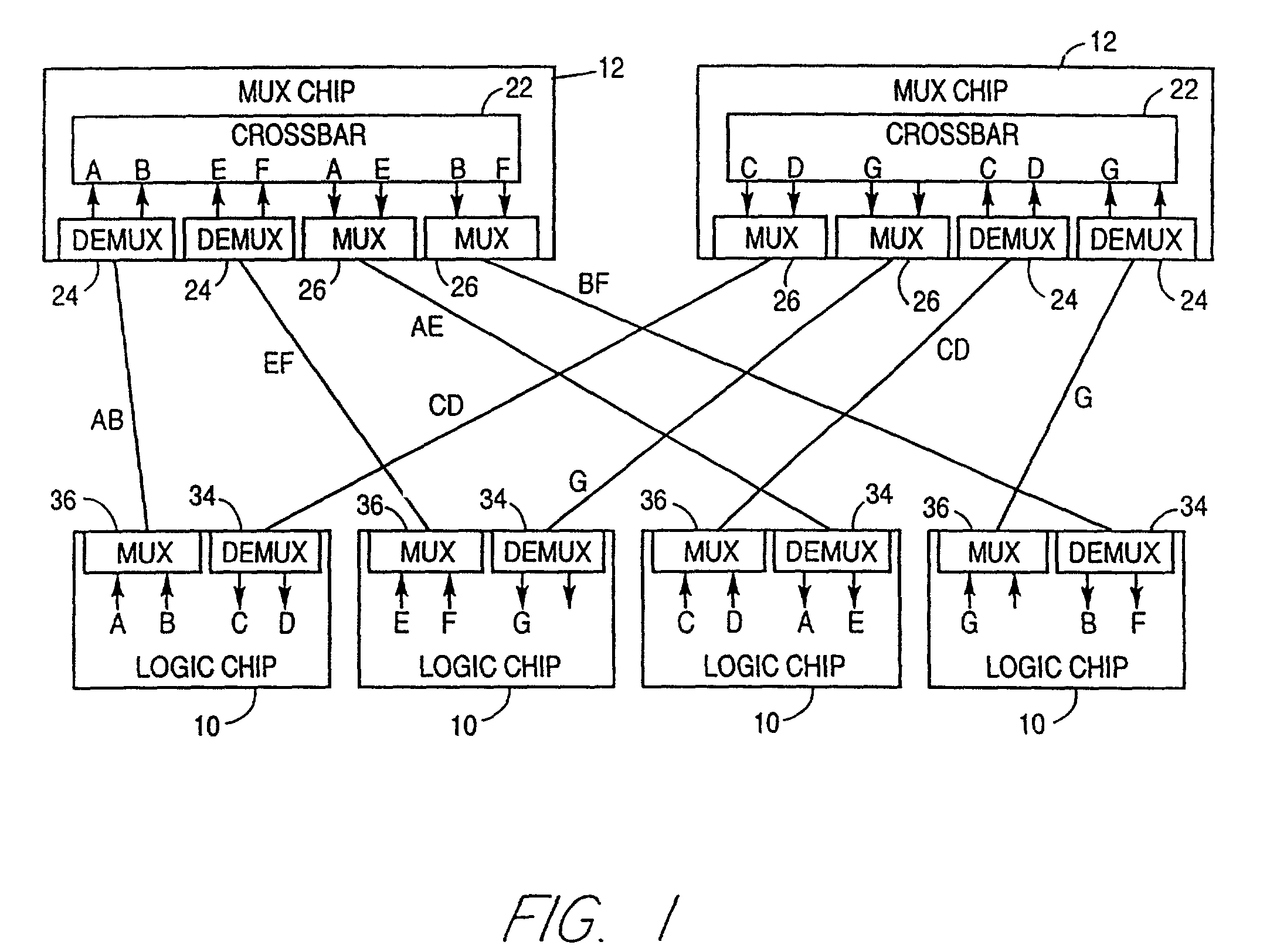
[0066]FIG. 1 shows a portion of the partial crossbar interconnect for a preferred embodiment of a hardware emulation system of the present invention. Embodiments of a partial crossbar interconnect architecture have been described in the U.S. Pat. Nos. 5,036,473, 5,448,496 and 5,452,231 by Butts et al, which are assigned to the same assignee as the present invention. The disclosure of U.S. Pat. Nos. 5,036,473, 5,448,496 and 5,452,231 are incorporated herein by reference in their entirety. In a partial crossbar interconnect, the input / output pins of each logic chip are divided into proper subsets, using the same division on each logic chip. The pins of each Mux chip (also known as crossbar chips) are connected to the same subset of pins from each logic chip. Thus, crossbar chip ‘n’ is connected to subset ‘n’ of each logic chip's...


PUM


Abstract

A hardware emulation system is disclosed which reduces hardware cost by time multiplexing multiple design signals onto physical logic chip pins and printed circuit board. The hardware emulation system comprises a plurality of reprogrammable logic devices, and a plurality of reprogrammable interconnect devices. The logic devices and interconnect devices are interconnected together such that multiple design signals share common I/O pins and circuit board traces through the use of multiplexing.

Description

[0001]This is a continuation of application Ser. No. 09 / 374,444, filed Aug. 13, 1999 and will issue as U.S. Pat. No. 6,377,912, which is a continuation of application Ser. No. 08 / 865,741 filed May 30, 1997 and issued as U.S. Pat. No. 5,960,191FIELD OF THE INVENTION[0002]The present invention relates in general to apparatus for verifying electronic circuit designs and more specifically to hardware emulation systems in which multiple design signals are carried on a single physical wire between programmable logic chips.BACKGROUND OF THE INVENTION[0003]Hardware emulation systems are devices designed for verifying electronic circuit designs prior to fabrication as chips or printed circuit boards. These systems are typically built from programmable logic chips (logic chips) and programmable interconnect chips (interconnect chips). The term “chip” as used herein refers to integrated circuits. Examples of logic chips include reprogrammable logic circuits such as field-programmable gate arra...

Claims


Application Information

Patent Timeline
IPC IPC(8): G06F17/50H04J99/00G06F9/455G01R31/317G01R31/28G06F11/22G06F11/26
CPCG01R31/2853G06F17/5027G01R31/31717Y10S370/916G06F30/331
Inventor SAMPLE, STEPHEN P.BERSHTEYN, MIKHAILBUTTS, MICHAEL R.BAUER, JERRY R.
Owner CADENCE DESIGN SYST INC
Why Eureka
Try Eureka