CMOS image sensor for improving the amount of light incident a photodiode

a technology of image sensor and photodiode, which is applied in the field of image sensor, can solve problems such as and achieve the effect of preventing interference and preventing loss of light focused quantity

Inactive Publication Date: 2010-06-22
DONGBU ELECTRONICS CO LTD
View PDF14 Cites 12 Cited by
  • Summary
  • Abstract
  • Description
  • Claims
  • Application Information

AI Technical Summary

Benefits of technology

[0015]An object of the present invention is to provide a CMOS image sensor that prevents interference between color segments of color filter arrays and also prevents a loss in the quantity of light focused on the photodiodes, and a fabricating method of the CMOS image sensor.

Problems solved by technology

However, the light that passes the blue, green, and red color segments can interfere with neighboring color segments, inducing a loss in the quantity of light that is focused on the photodiodes through dispersion and diffraction of the light passing through the segments of the color filter.

Method used


Image

  • CMOS image sensor for improving the amount of light incident a photodiode
  • CMOS image sensor for improving the amount of light incident a photodiode
  • CMOS image sensor for improving the amount of light incident a photodiode

Examples


Embodiment Construction

[0024]Reference will now be made in detail to a CMOS image sensor and a method of fabricating the same, according to preferred embodiments of the present invention, examples of which are illustrated in the accompanying drawings. Wherever possible, the same reference numbers will be used throughout the drawings to refer to the same or like parts.

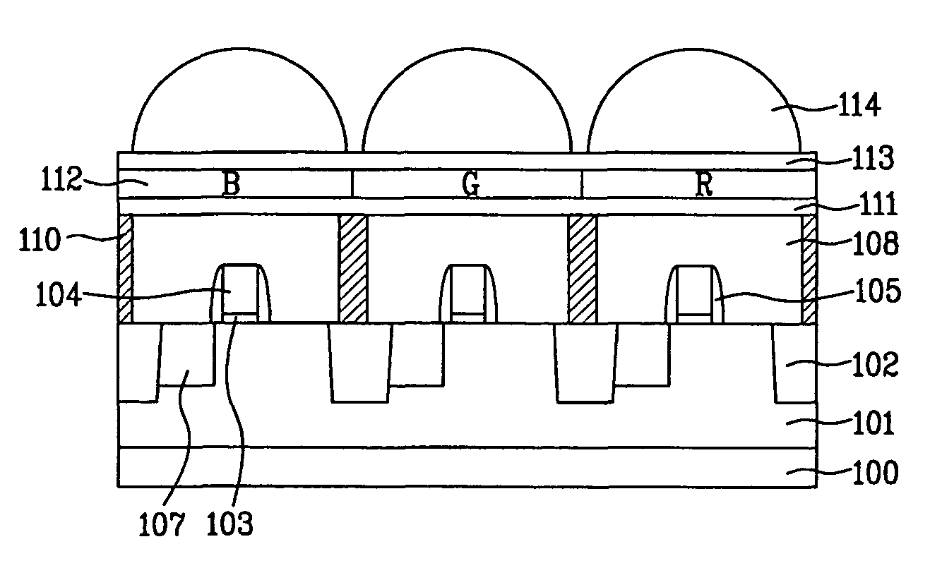
[0025]FIG. 2 is a sectional view of a CMOS image sensor according to an embodiment of the present invention.

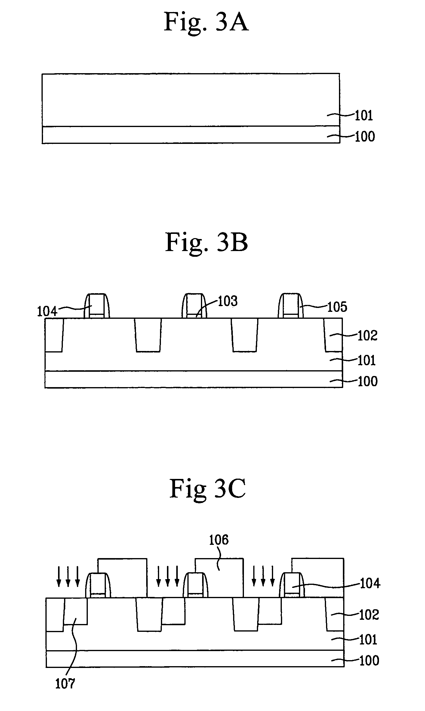
[0026]Referring to FIG. 2, a p-type epitaxial layer 101 can be formed on a p-type semiconductor substrate 100 having device isolation regions and active regions. A device isolation layer 102 can be formed on the device isolation regions of the semiconductor substrate 100, and gate electrodes 104 can be formed on the active regions of the semiconductor substrate 100 with a gate insulating layer 103 interposed therebetween. Insulating layer sidewalls 105 can be formed on the sides of gate electrodes 104. A plurality of n-type diffusion re...


PUM


Abstract

Provided are a CMOS image sensor and a fabricating method thereof. The CMOS image sensor includes a device isolation layer, a plurality of photodiode regions, an interlayer insulating layer, a refracting layer, a planarizing layer, a color filter layer, and a plurality of microlenses. The refracting layer, with a higher refractive index than that of the interlayer insulating layer, is formed through the interlayer insulating layer on portions of the device isolation layer, to divide the interlayer insulating layer and give the divided portions thereof the characteristics of a waveguide.

Description

RELATED APPLICATION[0001]This application claims the benefit under 35 U.S.C. §119(e), of Korean Patent Application Number 10-2005-0083669 filed Sep. 8, 2005, which is incorporated herein by reference in its entirety.FIELD OF THE INVENTION[0002]The present invention relates to an image sensor and a method of fabricating the same, and more particularly, to a complementary metal oxide semiconductor (CMOS) image sensor capable of preventing loss of light reaching a photodiode, while reducing interference between light waves, and a method of fabricating the CMOS image sensor.BACKGROUND OF THE INVENTION[0003]In general, an image sensor is a semiconductor device that converts an optical image into an electrical signal. Image sensors can largely be divided into charge coupled devices (CCD) and CMOS image sensors.[0004]Using CMOS fabricating technology, a CMOS image sensor can be fabricated using a simple fabrication process that consumes a relatively small amount of power and consists of a ...

Claims


Application Information

Patent Timeline
Patent Type & Authority Patents(United States)
IPC IPC(8): H01L31/062
CPCH01L27/14625H01L27/14685H01L27/1463H01L27/146
Inventor JUNG, SUN WOOK
Owner DONGBU ELECTRONICS CO LTD
Why Eureka
Try Eureka