Stressor for engineered strain on channel

a strainer and strain technology, applied in the direction of thin material processing, semiconductor devices, electrical devices, etc., can solve the problems of non-substitutional doping and complex substitutional doping in the pla

Active Publication Date: 2010-07-20
ASM IP HLDG BV
View PDF215 Cites 40 Cited by
  • Summary
  • Abstract
  • Description
  • Claims
  • Application Information

AI Technical Summary

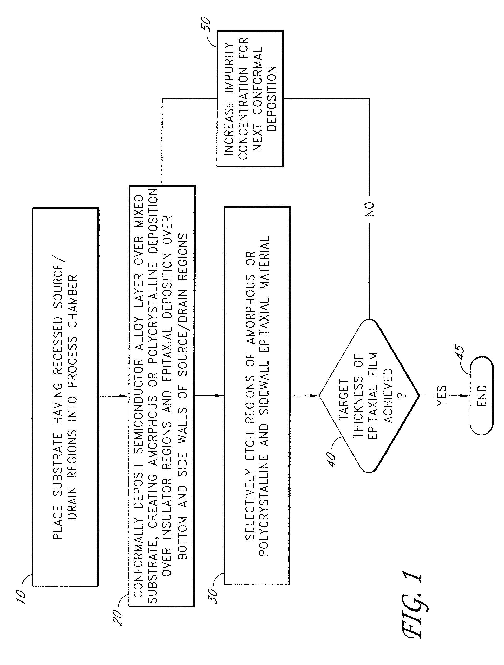
Problems solved by technology

However, in practice in situ substitutional doping is complicated by the tendency for the dopant to incorporate non-substitutionally during deposition, for example, by incorporating interstitially in domains or clusters within the silicon rather than by substituting for silicon atoms in the lattice structure.
Non-substitutional doping complicates, for example, carbon doping of silicon, carbon doping of silicon germanium, and doping of semiconductors with electrically active dopants.

Method used


Image

  • Stressor for engineered strain on channel
  • Stressor for engineered strain on channel
  • Stressor for engineered strain on channel

Examples


Embodiment Construction

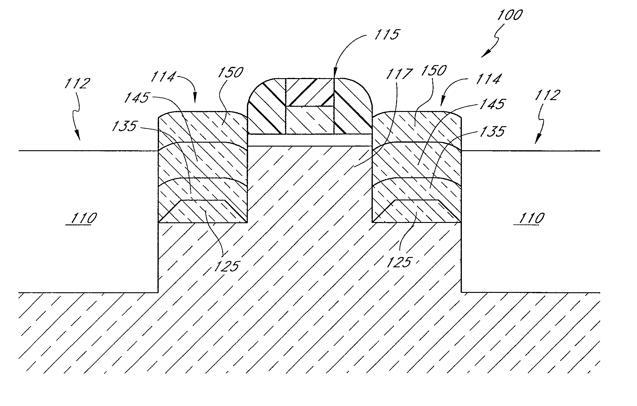
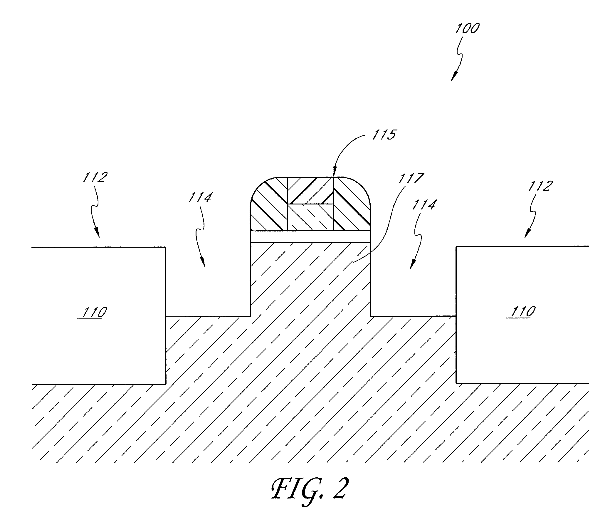
[0024]The term “impurity” is used herein to refer to additives, such as germanium or carbon, that alter the semiconductor lattice constant relative to silicon alone; the resultant semiconductor compound is often referred to as an alloy, or simply as a heteroepitaxial layer. “Dopants” can refer to either impurities or electrical dopants, such as phosphorous, arsenic, boron, or the like. The term “silicon-containing material” and similar terms are used herein to refer to a broad variety of silicon-containing materials, including without limitation, silicon (including crystalline silicon), carbon-doped silicon (“Si:C”), silicon germanium (“SiGe”), and carbon-doped silicon germanium (“SiGe:C”). As used herein, “carbon-doped silicon”, “Si:C”, “silicon germanium”, “SiGe,”“carbon-doped silicon germanium”, “SiGe:C” and similar terms refer to materials that contain the indicated chemical elements in various proportions and, optionally, minor amounts of other elements. For example, “silicon g...


PUM


Abstract

A semiconductor substrate having recesses filled with heteroepitaxial silicon-containing material with different portions having different impurity concentrations. Strained layers can fill recessed source / drain regions in a graded, bottom-up fashion. Layers can also line recess sidewalls with one concentration of strain-inducing impurity and fill the remainder to the recess with a lower concentration of the impurity. In the latter case, the sidewall liner can be tapered.

Description

FIELD OF THE INVENTION[0001]This invention relates generally to the deposition of silicon-containing materials in semiconductor processing, and relates more specifically to epitaxial deposition of silicon-containing materials in recessed source and drain regions of semiconductor substrates.BACKGROUND OF THE INVENTION[0002]In forming integrated circuits, epitaxial layers are often desired in selected locations, such as active area mesas among field isolation regions, or even more particularly over defined source and drain regions. While non-epitaxial material, which can be amorphous or polycrystalline, can be selectively removed from over the field isolation regions after deposition, it is typically considered more efficient to simultaneously provide chemical vapor deposition (“CVD”) and etching chemicals, and to tune conditions to result in zero net deposition over insulating regions and net epitaxial deposition over exposed semiconductor windows. This process, known as selective ep...

Claims


Application Information

Patent Timeline
Patent Type & Authority Patents(United States)
IPC IPC(8): H01L21/336
CPCH01L21/02381H01L21/02447H01L21/0245H01L21/02529H01L21/02532H01L29/0847H01L29/165H01L29/66636H01L29/78H01L29/7848H01L21/02639Y10T428/2462H01L21/18H01L21/20H01L21/205
Inventor THOMAS, SHAWNTOMASINI, PIERRE
Owner ASM IP HLDG BV
Why Eureka
Try Eureka