Data transmission system

a data transmission system and data technology, applied in the field of data transmission systems, can solve the problems of reducing the effective communication speed, unable to realize the correction of offset voltage fluctuations, and exacerbate the false detection rate of low-amplitude high-speed received data, so as to prevent the increase or decrease of the circuit scal

Inactive Publication Date: 2010-08-03
NEC CORP
View PDF13 Cites 3 Cited by
  • Summary
  • Abstract
  • Description
  • Claims
  • Application Information

AI Technical Summary

Benefits of technology

[0011]It is an object of the present invention to provide a data transmission system that can correct offset voltage while receiving signals.
[0014]In a data transmission system such as described hereinabove, the offset voltage of the signal detection circuit is corrected in the reception circuit based on the abundance ratio of each value of the data sequence transmitted from the transmission circuit, as a result, the offset voltage of the signal detection circuit can be corrected while signals are being received. In addition, the offset voltage is corrected using a data sequence that is transmitted, whereby fluctuations in the offset voltage of the signal detection circuit that occur during transmission of data can also be corrected. Still further, increase in the circuit scale or decrease of the communication speed can be prevented because there is no need for circuits for generating a dedicated training sequence or an adjustment pattern for correcting the offset voltage of the signal detection circuit.

Problems solved by technology

As previously described, the input difference in potential that can be detected in a signal detection circuit is determined by the offset voltage, and the problem therefore arises that the false detection rate of data of low-amplitude high-speed received signals is exacerbated by the offset voltage.
There is a further problem that the self-test for correcting the offset voltage of the above-described signal detection circuit is implemented during operations for system initialization, and correction therefore cannot be realized for fluctuations of the offset voltage generated by such factors as the temperature fluctuations during use of the system.
However, the implementation of self-testing prevents the reception of signals in the signal detection circuit and the inability to send information results in a decrease of the effective communication speed.

Method used


Image

  • Data transmission system
  • Data transmission system
  • Data transmission system

Examples


first embodiment

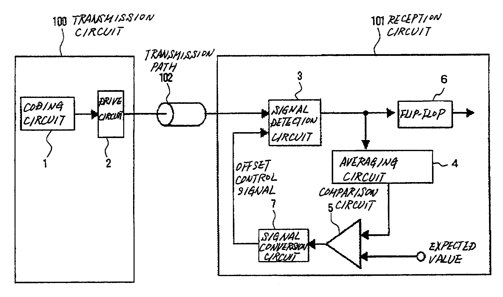
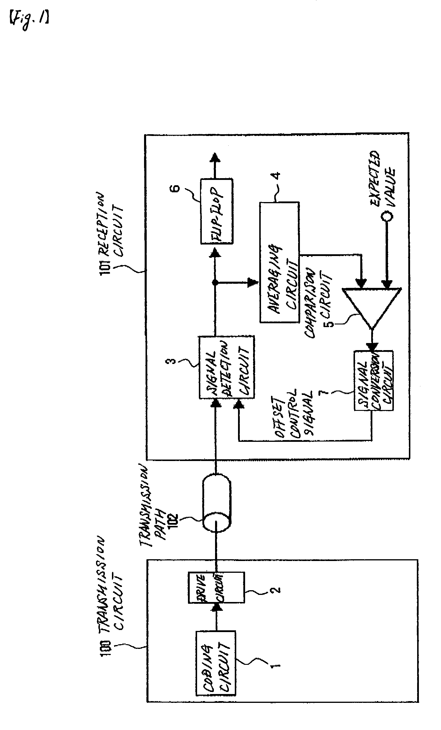
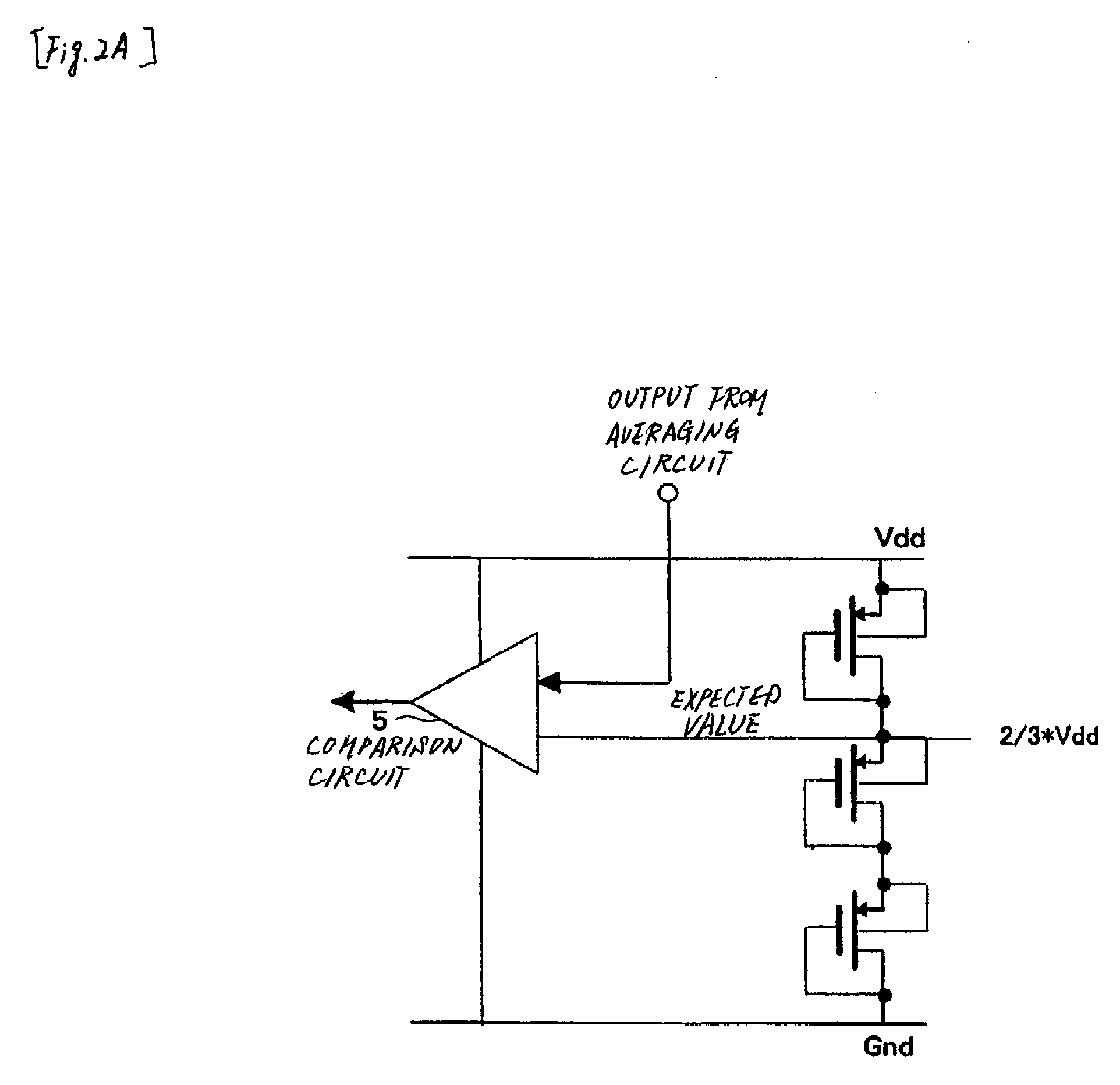
[0032]As shown in FIG. 1, the data transmission system of the first embodiment includes transmission circuit 100 for encoding and transmitting a data sequence that is the object of transmission and reception circuit 101 that is provided with a signal detection circuit for detecting a data sequence from a received signal.

[0033]Transmission circuit 100 is provided with: coding circuit 1 for encoding a data sequence that is the object of transmission and drive circuit 2 for transmitting the encoded data sequence to transmission path 102.

[0034]Coding circuit 1 encodes a data sequence that is the object of transmission such that the proportion of each value that exists in each prescribed data length is fixed. For example, in binary transmission, encoding is carried out such that the abundance ratios of the two values “1” and “0” are, for example: 1:1 or 2:1. In quaternary transmission, encoding is carried out such that the abundance ratios of the four values “11,”“10,”“01,” and “00” are,...

second embodiment

[0065]In the second embodiment, an example is shown in which averaging circuit 4 and comparison circuit 5 that belong to reception circuit 101 of the first embodiment shown in FIG. 1 are realized by digital signal processing.

[0066]As shown in FIG. 9, the functions of averaging circuit 4 and comparison circuit 5 can be realized by digital signal processing by, upon reception of a data sequence in which the abundance ratio of “1” and “0” realized by encoding is 1:1, counting either one of “1” and “0” that are detected from the received signal by counter 16 and comparing in comparison circuit 5 to determine if this value is greater than one-half the data length used in averaging.

[0067]When coding circuit 1 carries out coding in which the occurrence ratio of “1” and “0” is m:n and the data length used in averaging is “1,” the expected value when “1” is counted in counter 16 is:

(m / (m+n))×1  (3)

and the expected value when “0” is counted in counter 16 is:

(n / (m+n))×1  (4)

[0068]FIG. 10 is an...

third embodiment

[0072]In the above-described first embodiment and second embodiment, methods were shown for correcting the offset voltage of signal detection circuit 3 when transmitting a data sequence by single-end transmission. In the third embodiment, a method is proposed for correcting offset voltage of signal detection circuit 3 when transmitting a data sequence by differential transmission. In the following explanation, an example is described in which, similar to the second embodiment, averaging circuit 4 and comparison circuit 5 that belong to reception circuit 101 are both realized by digital signal processing. However, the third embodiment can also be applied to a configuration in which averaging circuit 4 and comparison circuit 5 are realized by analog circuits, as shown in the first embodiment.

[0073]As shown in FIG. 12, because a data sequence is transmitted by a differential signal, the data transmission system of the third embodiment is of a configuration in which the drive circuit in...


PUM


Abstract

A data transmission system is made up from: a transmission circuit (100) for generating and transmitting a data sequence in which the abundance ratio of each value for each prescribed data length is fixed, and a reception circuit (101) for, based on the abundance ratio of each value of a data sequence transmitted from the transmission circuit (100), correcting the offset voltage of a signal detection circuit (3) that detects values of the data sequence.

Description

CROSS-RELATED REFERENCE APPLICATIONS[0001]This application is a 371 of PCT / JP2006 / 315917 filed on Aug. 11, 2006, which claims the benefit of foreign priority of Japanese Patent Application Number 2005-259354, filed on Sep. 7, 2005.TECHNICAL FIELD[0002]The present invention relates to a data transmission system provided with a signal detection circuit for detecting, from a signal received by way of a transmission path, data contained in the signal.BACKGROUND ART[0003]A plurality of transistors that have been produced on the same silicon chip have all been produced under exactly the same conditions and therefore have characteristics such as threshold voltage and mutual conductance that are essentially matched. As a result, a balanced-input circuit that uses transistors is ideal for detecting a microsignal, and components such as differential amplification circuits and differential sampling latch circuits are frequently used in the input stage of a signal detection circuit for detectin...

Claims


Application Information

Patent Timeline
Patent Type & Authority Patents(United States)
IPC IPC(8): H03M1/12
CPCH04L25/028H04L25/063
Inventor SUNAGA, KAZUHISA
Owner NEC CORP
Why Eureka
Try Eureka