Video processing circuit and method, liquid crystal display apparatus, and electronic apparatus

a video processing circuit and liquid crystal display technology, applied in the field of video processing circuit and method, liquid crystal display apparatus, electronic apparatus, can solve the problems of display faults, etc., to prevent an increase in the scale and complexity of video processing circuits and reduce the occurrence of display faults.

Active Publication Date: 2014-08-26
SEIKO EPSON CORP
View PDF12 Cites 0 Cited by
  • Summary
  • Abstract
  • Description
  • Claims
  • Application Information

AI Technical Summary

Benefits of technology

[0009]An advantage of some aspects of the invention is to provide a technology capable of preventing an increase in scale and complexity and the like of a video processing circuit and reducing the occurrence of display faults caused by reverse tilt domain.
[0010]According to one aspect of the invention, there is provided a video processing circuit, which includes a liquid crystal panel provided with pixel electrodes provided on a first substrate, a common electrode provided on a second substrate, and liquid crystal elements having liquid crystal interposed between the pixel electrodes and the common electrode, and designates an applied voltage, which is applied to the liquid crystal elements, to the liquid crystal panel based on a video signal, including: a boundary detection unit that detects a specific boundary (a risk boundary), which is a part of a boundary of a first pixel for which an applied voltage designated by the video signal is less than a first voltage, and a second pixel for which the applied voltage is more than a second voltage larger than the first voltage, the specific boundary being determined by tilt azimuth of the liquid crystal; and a replacement unit that replaces an applied voltage to a liquid crystal element corresponding to the first pixel with a predetermined voltage from the applied voltage designated by the input video signal when the applied voltage designated by the video signal is less than a third voltage which is smaller than the first voltage with respect to the first pixel adjacent to the specific boundary. According to one aspect of the invention, since only a process for detecting the boundary and the specific boundary among pixels, rather than the entire image corresponding to one frame, is performed, an increase in the scale and complexity of the video processing circuit can be prevented, as compared with the configuration in which an image corresponding to two frames or more is analyzed and the movement of the image is detected.
[0014]According to a further aspect of the invention, when an applied voltage designated by a video signal of the pixel is less than the third voltage with respect to one or more pixels which are adjacent at an opposite side of the risk boundary with respect to the first pixel adjacent to the specific boundary and continuous toward a direction opposite to that of the specific boundary, the replacement unit may replace an applied voltage to a liquid crystal element corresponding to the pixel with the third voltage from the applied voltage designated by the video signal. With such a configuration, even when a response time of a liquid crystal element is longer than a time interval in which a display screen is updated, the occurrence of reverse tilt domain can be prevented.
[0015]In detail, when a time interval in which the display of the liquid crystal panel is updated is defined as S and a response time of the liquid crystal element when an applied voltage is switched to the third voltage from a voltage less than the third voltage is defined as T, if S<T, the number of one or more pixels, which are adjacent at an opposite side of the specific boundary with respect to the first pixel adjacent to the specific boundary and continuous toward a direction opposite to that of the specific boundary, may have a value of an integer part of a value obtained by dividing the response time T by the time interval S. If such a value is employed, it is not necessary to replace a grayscale designated by a video signal Vid-in, and the unstable state of liquid crystal molecules can be prevented from being continuous even at the time of the next update (rewriting).

Problems solved by technology

For example, if a transverse electric field is applied to liquid crystal of a vertical alignment (VA) mode, a twisted nematic (TN) mode and the like to be driven by a longitudinal electric field, since alignment failure (reverse tilt) of the liquid crystal occurs, display faults may occur.
However, in the above technology, since video signals need to be analyzed for each frame, this may cause an increase in the scale and complexity of a video processing circuit.

Method used


Image

  • Video processing circuit and method, liquid crystal display apparatus, and electronic apparatus
  • Video processing circuit and method, liquid crystal display apparatus, and electronic apparatus
  • Video processing circuit and method, liquid crystal display apparatus, and electronic apparatus

Examples


embodiment

[0047]Hereinafter, an embodiment of the present invention will be described with reference to the accompanying drawings.

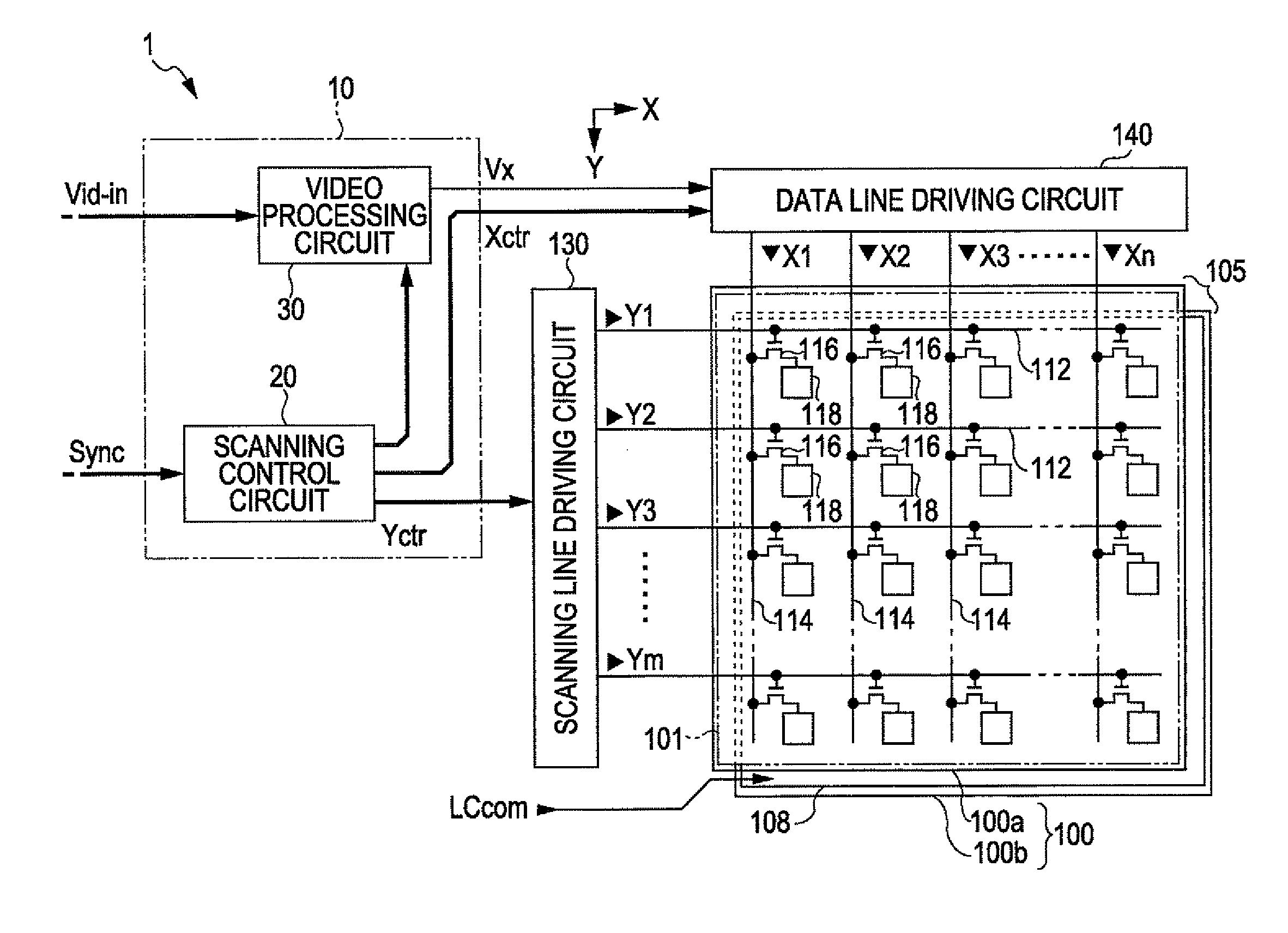
[0048]FIG. 1 is a block diagram showing the entire configuration of a liquid crystal display apparatus to which a video processing circuit according to the embodiment is applied.

[0049]As shown in FIG. 1, the liquid crystal display apparatus 1 includes a control circuit 10, a liquid crystal panel 100, a scanning line driving circuit 130, and a data line driving circuit 140.

[0050]Among them, the control circuit 10 receives video signals Vid-in from an upper apparatus in synchronization with a synchronization signal Sync. The video signals Vid-in are digital data for designating grayscale levels of each pixel in the liquid crystal panel 100, and are supplied in a scanning sequence according to a vertical scanning signal, a horizontal scanning signal and a dot clock signal (not shown) included in the synchronization signal Sync.

[0051]In addition, since the video signal...


PUM


Abstract

The video processing circuit includes a boundary detection unit that detects a specific boundary, which is a part of a boundary of a first pixel for which an applied voltage designated by the video signal is less than a first voltage, and a second pixel for which the applied voltage is more than a second voltage larger than the first voltage, the specific boundary being determined by tilt azimuth of the liquid crystal, and a replacement unit that replaces an applied voltage to a liquid crystal element corresponding to the first pixel with a predetermined voltage from the applied voltage designated by the input video signal when the applied voltage designated by the video signal is less than a third voltage smaller than the first voltage with respect to the first pixel adjacent to the specific boundary.

Description

BACKGROUND[0001]1. Technical Field[0002]The present invention relates to a technology capable of reducing display faults in a liquid crystal panel.[0003]2. Related Art[0004]A liquid crystal panel has a configuration in which liquid crystal is interposed between a pair of substrates spaced apart from each other by a constant gap.[0005]In detail, in the liquid crystal panel, liquid crystal is interposed between a first substrate, in which pixel electrodes are arranged for each pixel in a matrix shape, and a second substrate in which a common electrode is disposed in common over all pixels, and liquid crystal elements are formed of the pixel electrodes, the liquid crystal and the common electrode. In the liquid crystal element, if a voltage according to a grayscale level between the pixel electrodes and the common electrode is applied and held, an alignment state of the liquid crystal is specified for each pixel, so that transmittance or reflectivity is controlled. Thus, in the above c...

Claims


Application Information

Patent Timeline
Patent Type & Authority Patents(United States)
IPC IPC(8): G09G3/36
CPCG09G3/3648G09G2330/08G09G2360/16
Inventor HOSAKA, HIROYUKIIISAKA, HIDEHITO
Owner SEIKO EPSON CORP
Why Eureka
Try Eureka