High resolution digital analog conversion circuit

a conversion circuit and high-resolution technology, applied in the field of high-resolution digital analog conversion circuits, can solve the problems of high monotonicity, high cost of converters with higher resolution, and generation of glitch effects by methods, etc., and achieve the effect of high monotonicity and high resolution

a conversion circuit and high-resolution technology, applied in the field of high-resolution digital analog conversion circuits, can solve the problems of high monotonicity, high cost of converters with higher resolution, and generation of glitch effects by methods, etc., and achieve the effect of high monotonicity and high resolution

US7773009B2Active Publication Date: 2010-08-10SPECS ZURICH

Image

  • High resolution digital analog conversion circuit
  • High resolution digital analog conversion circuit

Examples


Embodiment Construction

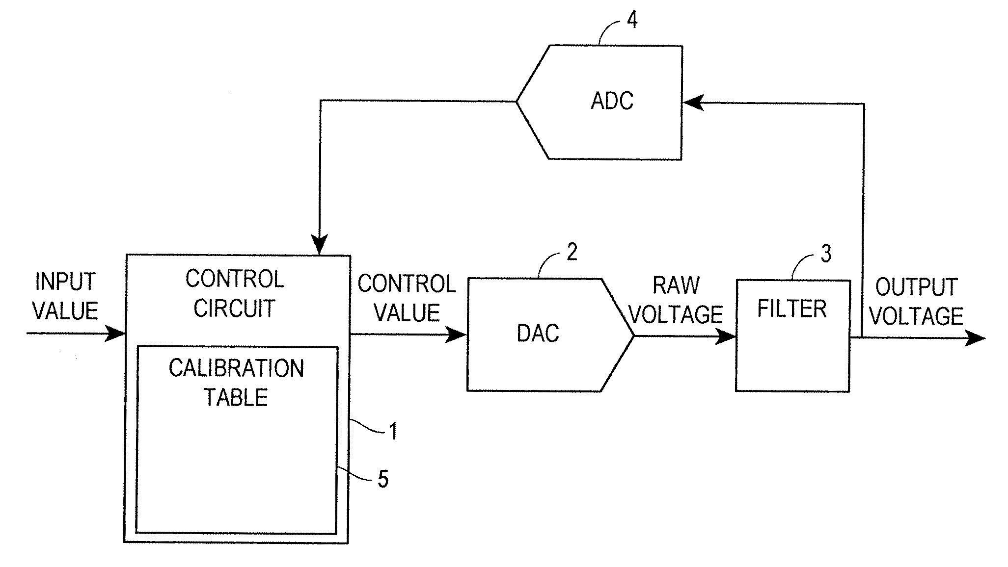
[0026]The digital analog conversion circuit of FIG. 1 comprises a control circuit 1 with an input for receiving an n bit input value, e.g. with n=20. Control circuit 1 generates a series of m bit control values, e.g. with m=16, and feeds the same to an m bit DAC 2. For each control value, DAC 2 generates the corresponding voltage, termed “raw voltage” in the following. The raw voltage is fed to a low pass filter 3 for generating the output voltage of the digital analog conversion circuit. The digital analog conversion circuit further comprises an analog digital converter (ADC) 4 that allows to measure the output voltage and feeds it back to control circuit 1 for calibration.

[0027]Control circuit 1 may be a programmable logic circuit, such as a FPGA.

[0028]The purpose of the device of FIG. 1 is to generate an output voltage vout as a function of the input value vi, i.e.

vout=f(vi)  (1)

with f typically being a linear function.

[0029]Operation of the device of FIG. 1 is as follows:

[0030]W...


PUM


Abstract

To increase the accuracy and resolution of an m bit digital analog converter, n bit input values with n>m are fed to a control circuit and converted to a series of control values for the digital analog converter using dithering techniques. When the series of control values straddles a major transition where a large number of bits are switched between 1 and 0, a corrected series of control values is retrieved from a calibration table. The corrected series takes into account the glitch effects observed at the output of digital analog converter at a major transition.

Description

CROSS REFERENCE RELATED APPLICATIONS[0001]This application claims the priority of European patent application 07008269.8, filed Apr. 24, 2007, the disclosure of which is incorporated herein by reference its entirety.BACKGROUND OF THE INVENTION[0002]The invention relates to a high resolution digital analog conversion circuit.[0003]Digital to analog converters (DAC) available today have usually up to 16 bit resolution. Converters with higher resolution tend to be expensive and / or are very slow.[0004]In some applications converters having a high precision and monotonicity are required. For example, nanopositioning and servo control applications require a high resolution DAC, with particularly high monotonicity. Typical requirements are for a DAC with a resolution and monotonicity of at least 20 bits and an analog bandwidth of at least 5 kHz.[0005]One way to increase the resolution is to use 16 bit conversion and to switch its value fed to the DAC between two adjacent 16 bit values, the...

Claims


Application Information

Patent Timeline
10 Aug 2010
Publication
US7773009B2
IPC
H03M1/10
CPC
H03M1/1042; H03M1/0863; H03M1/661
Inventors
RYCHEN, JORG