Switching control system and motor driving system

a technology of switching control system and motor driving, which is applied in the direction of electronic commutators, pulse techniques, dynamo-electric converter control, etc., can solve the problems of low switching speed, possible destruction or disturbance of other electronic equipment, and malfunctioning or destroying elements, etc., and achieve linear slew rate, linear slew rate, and easy setting

Inactive Publication Date: 2010-08-17
PANASONIC SEMICON SOLUTIONS CO LTD
View PDF6 Cites 0 Cited by
  • Summary
  • Abstract
  • Description
  • Claims
  • Application Information

AI Technical Summary

Benefits of technology

[0076]According to the present invention, in the turn-on operation of the high-side output transistor, while the output voltage of the high-side output transistor is rising, the clip control allows the control terminal of the output transistor to be charged with a current of a given value. The present invention can thus provide a very linear slew rate for the output voltage. In the turn-off operation of the high-side output transistor, while the output voltage of the high-side output transistor is dropping, the clip control allows the control terminal of the output transistor to discharge a current of a given value. The present invention can thus provide a very linear slew rate for the output voltage.
[0077]A clip circuit does not require any complicated control but requires only a small circuit scale. The values of the charging current and discharging current can be easily set using a clip voltage and resistance. This eliminates the need for an external input terminal for current setting.
[0078]This means that the present invention can prevent an increase in circuit scale and in the number of terminals, reduce the price and size of the system, and be applied to output transistors made in accordance with various specifications.

Problems solved by technology

With the output transistors, too high a switching speed for the turn-on or turn-off operation may rapidly vary voltage to cause elements to malfunction or be destroyed.
Furthermore, such a switching speed may pose a problem such as possible destruction or the possible disturbance of other electronic apparatuses due to noise.
In contrast, too low a switching speed may pose a problem such as operational errors resulting from possible delay or the increased amount of generated heat resulting from increased losses.
The known common configurations disadvantageously have difficulty setting the slew rate of an output voltage from the high-side output transistor (node 28).
Specifically, in FIGS. 18 and 19, since the slew rate is high immediately after t2, disadvantageously the voltage may vary rapidly to cause malfunctioning or destruction of elements and noise may be generated to disturb other electronic apparatuses.
Immediately before t3, the low slew rate may pose a problem such as operational errors resulting from possible delay or the increased amount of generated heat resulting from increased losses, during switching.
This means that it is difficult to set the slew rate at a well-balanced value.
This complicates controllability and increases the scale of the circuit.
This in turn prevents the use of more inexpensive small-sized packages.
This may inhibit a reduction in the price and size of the switching control system.

Method used


Image

  • Switching control system and motor driving system
  • Switching control system and motor driving system
  • Switching control system and motor driving system

Examples


embodiment 1

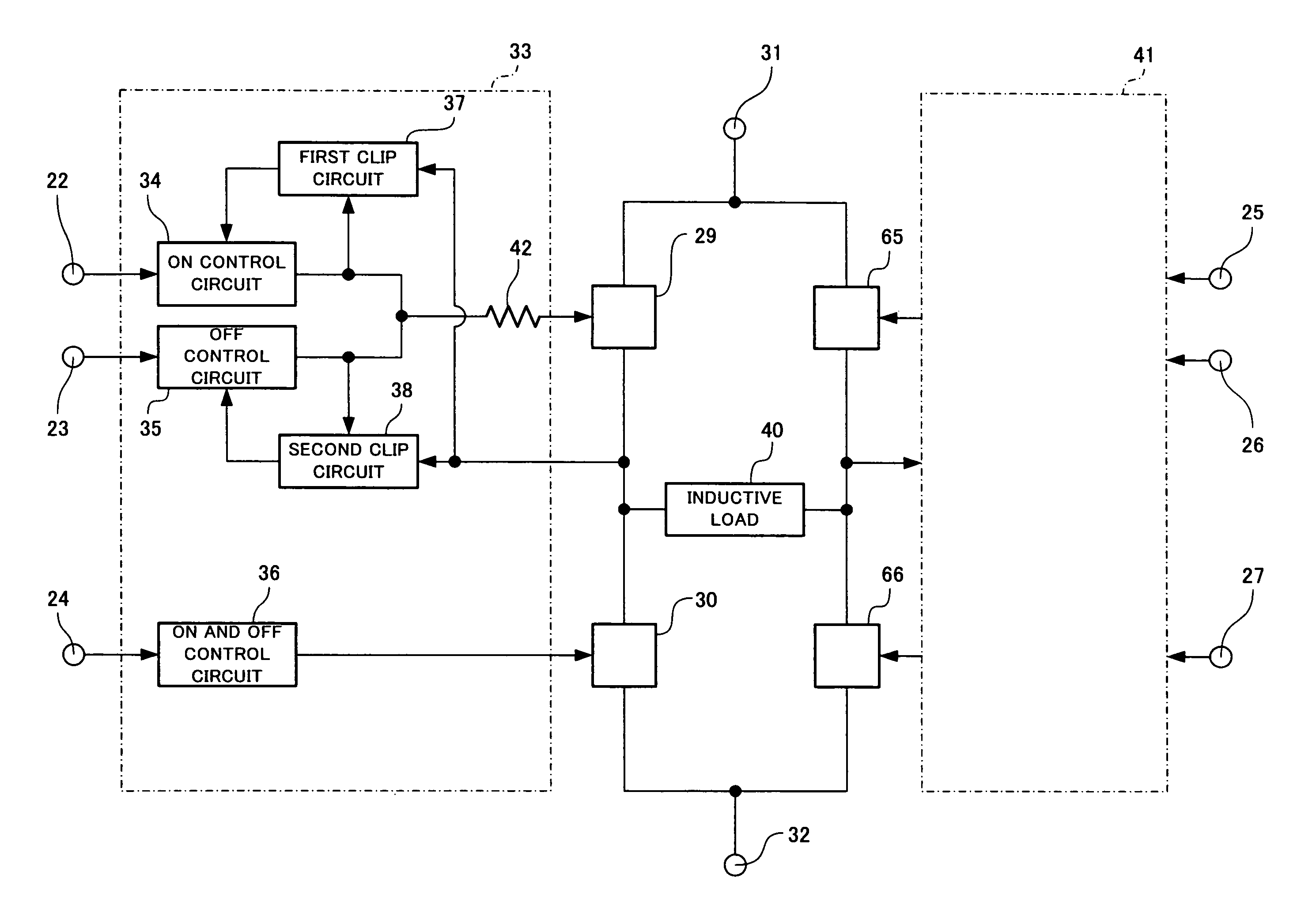
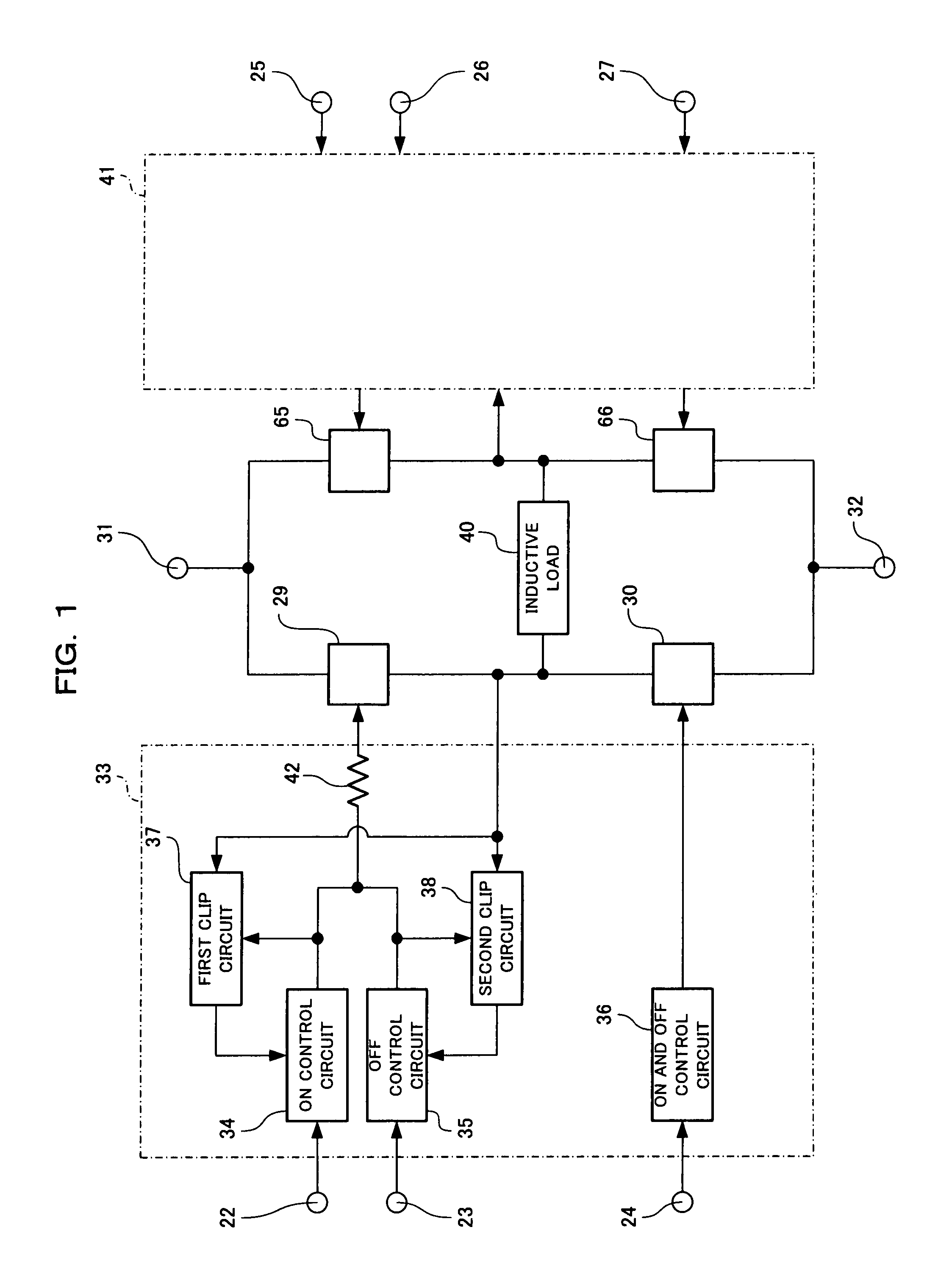
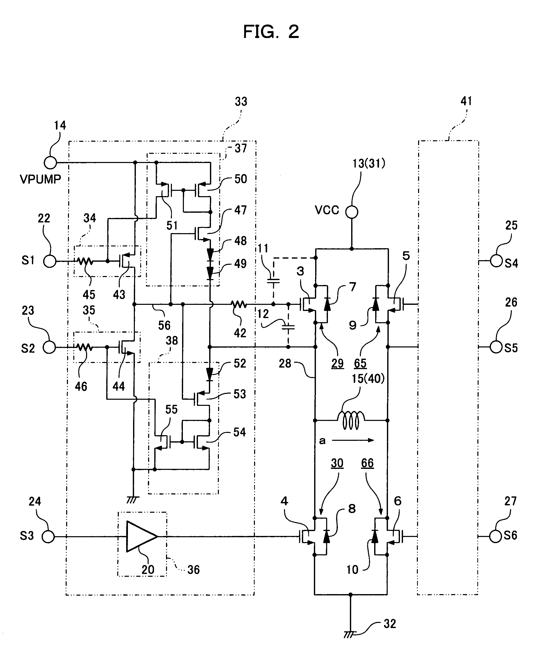
[0099]FIG. 1 shows a block diagram of Embodiment 1 of the present invention. Reference numerals 29 and 30 denote a first output transistor and a second output transistor. The output transistors 29 and 30 and output transistors 65 and 66 constitute an output circuit. Reference numerals 31 and 32 denote a first power supply terminal and a second power supply terminal, respectively, which are connected to the output circuit. Reference numeral 33 denotes a predrive circuit that drives the output transistors 29 and 30. Reference numeral 41 denotes a predrive circuit that drives the output transistors 65 and 66. Reference numeral 40 denotes an inductive load driven by the output circuit. The output transistors 29 and 30 are N-type MOS transistors. A drain terminal of the first output transistor 29 is connected to the first power supply terminal 31. A source terminal of the first output transistor 29 is connected to a drain terminal of the second output transistor 30. A source terminal of ...

embodiment 2

[0152]FIG. 7 shows a circuit diagram of Embodiment 2 of the present invention. FIG. 7 shows a configuration corresponding to that of Embodiment 1 to which a resistor 57 is added. In the configuration in FIG. 7, the clip voltage setting circuit in the first clip circuit 37 is composed of the diodes 48 and 49 and the resistor 57. The clip voltage setting circuit in the second clip circuit 38 is composed of the diode 52 and the resistor 57. The resistor 57 is connected between the diode 49 and the diode 52 and the node 28. The remaining part of the configuration is the same as that of Embodiment 1, shown in FIG. 2, and will thus not be described below.

[0153]In the configuration according to Embodiment 1, the first clip voltage, determined by the first clip circuit 37, is the fixed plus voltage V1clip. During the clip control, the current I1clip flows from the cathode of the diode 49 toward the node 28. In contrast, in the configuration according to Embodiment 2, shown in FIG. 7, the re...

embodiment 3

[0157]FIG. 8 shows a circuit diagram of Embodiment 3 of the present invention. FIG. 8 shows a configuration corresponding to that of Embodiment 1 to which diodes 59 and 60 and resistors 61 and 62 are added. In the configuration in FIG. 8, the clip voltage setting circuit in the first clip circuit 37 is composed of the diodes 48, 49, and 59 and the resistor 61 and connected to the node 28. The clip voltage setting circuit in the second clip circuit 38 is composed of the diodes 52 and 60 and the resistor 62 and connected to the node 28.

[0158]In Embodiment 3, when a forward breakdown voltage for the diode 59 is defined as V59d and the internal impedance of the diode 59 is sufficiently low compared to that of the resistor 61 and is negligible, the first clip voltage for the node 56 with respect to the voltage of the node 28 can be set equal to {V1clip+V59d+(I1clip*R61)}.

[0159]When a forward breakdown voltage for the diode 60 is defined as V60d and the internal impedance of the diode 60 ...


PUM


Abstract

The present invention inexpensively controls a turn-on and turn-off switching speed for MOS transistors made in accordance with various specifications. According to the present invention, during an output voltage rise period for a turn-on operation of the MOS transistor, a fixed current determined by a first clip circuit and a resistor is input to a gate terminal of the MOS transistor to obtain a linear rise slew rate. During an output voltage drop period for a turn-off operation of the MOS transistor, a fixed current determined by a second clip circuit 38 and a resistor is input to the gate terminal of the MOS transistor to obtain a linear drop slew rate.

Description

[0001]The present application claims priority to Japanese Patent Applications No. 2007-232118, filed Sep. 7, 2007, the entire contents of which are expressly incorporated by reference.FIELD OF THE INVENTION[0002]The present invention relates to a motor driving system, and in particular, to a switching control system that performs PWM (Pulse Width Modulation).BACKGROUND OF THE INVENTION[0003]PWM driving is a method of turning on or off output transistors connected to an inductive load for a motor and varying the ratio of turned-on transistors to turned-off transistors to control the amount of power supplied to the inductive load. The PWM driving is well known as a power-saving driving method. MOSFETs are commonly used as the output transistors connected to the inductive load for the motor. A predrive circuit is required to drive control terminals for the output transistors.[0004]With the output transistors, too high a switching speed for the turn-on or turn-off operation may rapidly ...

Claims


Application Information

Patent Timeline
Patent Type & Authority Patents(United States)
IPC IPC(8): H02P6/14H02M7/48H03K17/04H03K17/687H03K17/695
CPCH02P27/08H03K17/08122H03K17/165H03K17/6871H03K17/731H03K17/08142H03K17/166H03K17/74H03K2017/0806
Inventor KURODA, KEISUKEMARUYAMA, KEN
Owner PANASONIC SEMICON SOLUTIONS CO LTD
Why Eureka
Try Eureka