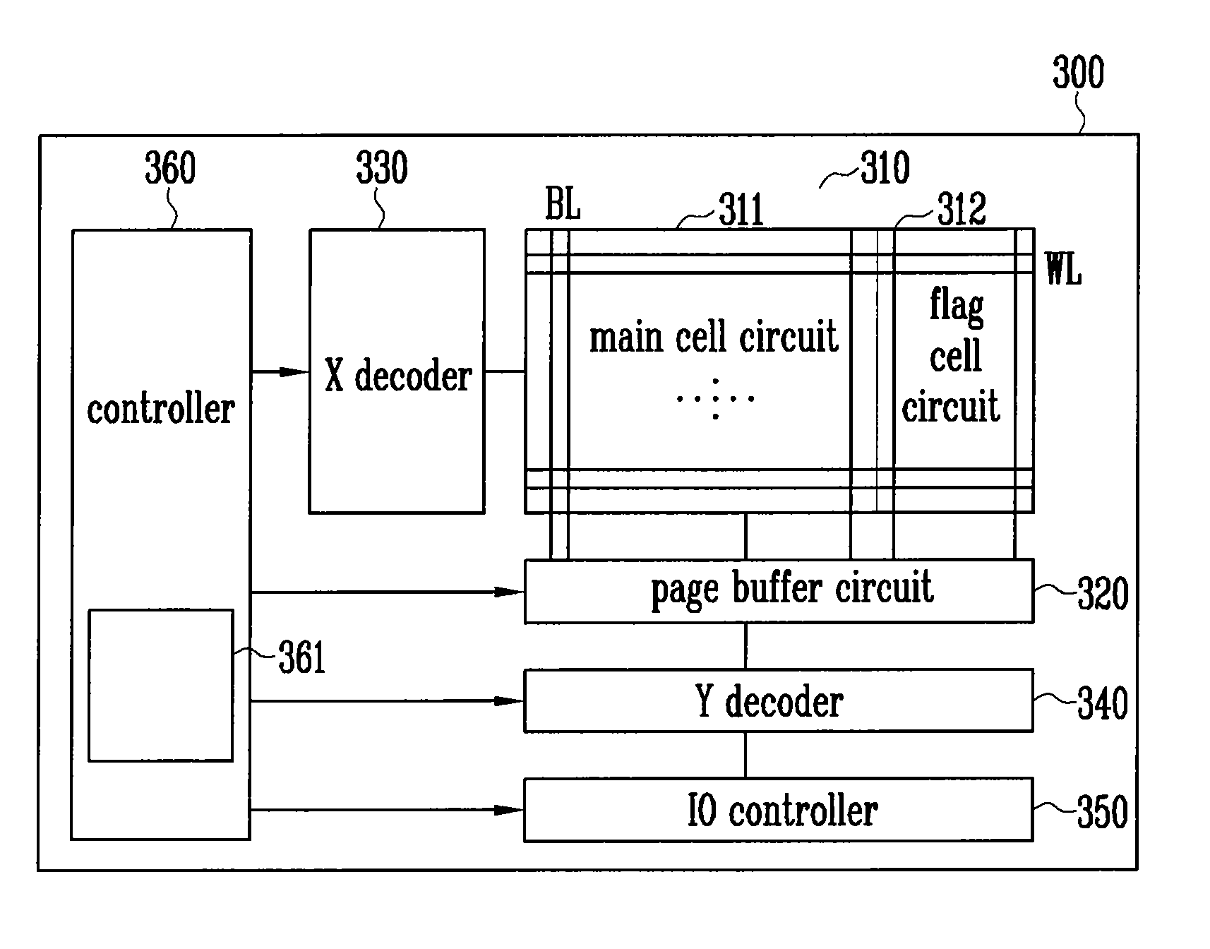
Page buffer, memory device having the page buffer and method of operating the same
a memory device and page buffer technology, applied in static storage, digital storage, instruments, etc., can solve the problems of affecting only one of the bits in the memory cell, interference effect may occur between, and the characteristics of adjacent memory cells may deteriorate, so as to minimize the shift of the threshold voltage distribution and minimize the error rate
- Summary
- Abstract
- Description
- Claims
- Application Information
AI Technical Summary
Benefits of technology
Problems solved by technology
Method used
Image

Examples
Embodiment Construction
[0036]Hereinafter, the preferred embodiments of the present invention will be explained in detail with reference to the accompanying drawings.
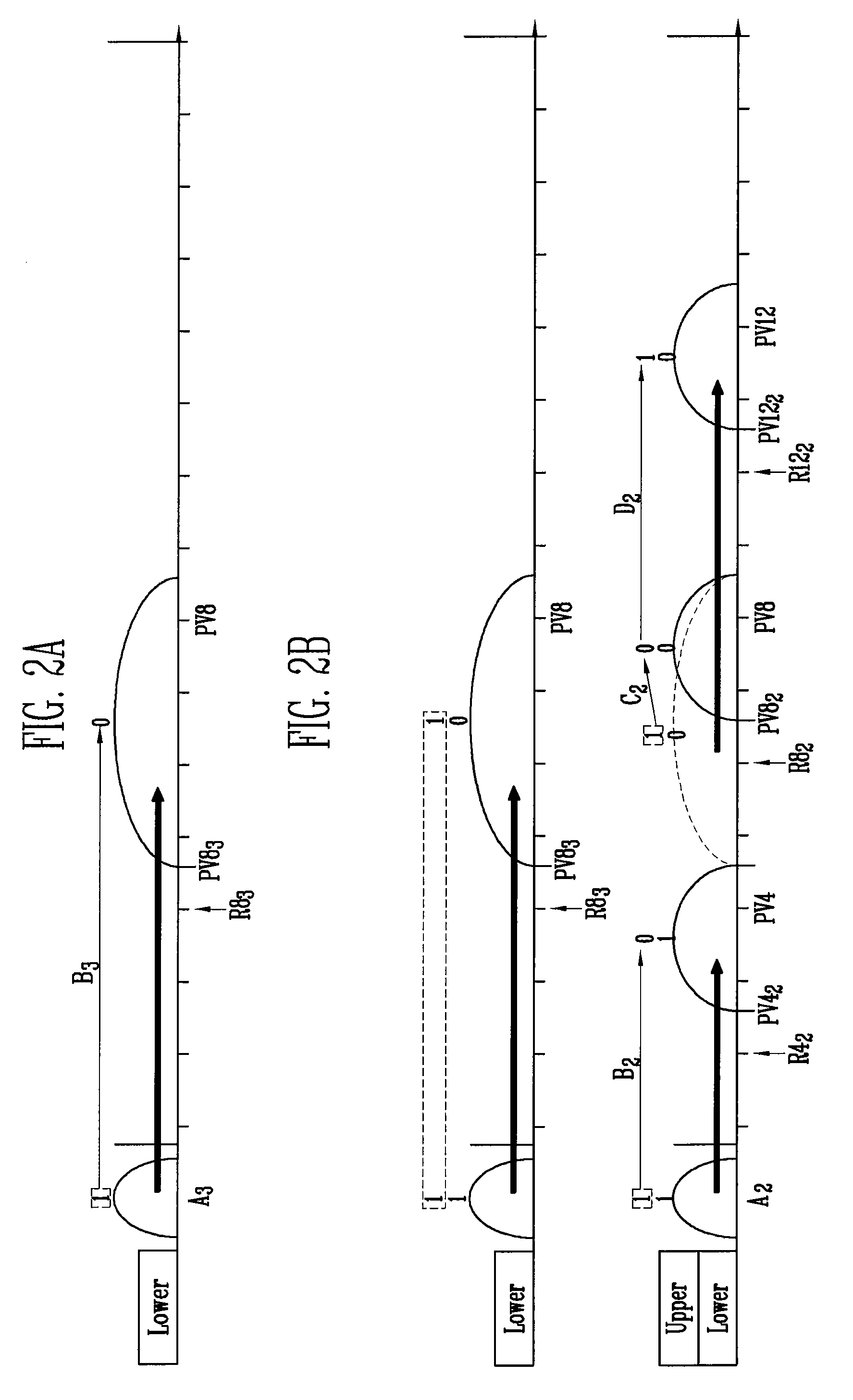
[0037]FIG. 2A to FIG. 2D are views illustrating a threshold voltage distribution in accordance with a program operation of MLC for storing 4 bits according to one example embodiment of the present invention. Particularly, FIG. 2A shows a shift of a threshold voltage distribution of a memory cell in accordance with a program of a first bit Lower of four bits, and FIG. 2B illustrates a shift of a threshold voltage distribution of the memory cell in accordance with a program of a second bit Upper of the bits. FIG. 2C shows a shift of a threshold voltage distribution of the memory cell in accordance with a program of a third bit Higher of the bits, and FIG. 2D illustrates a shift of a threshold voltage distribution of the memory cell in accordance with a program of a fourth bit Top of the bits.
[0038]In FIG. 2A, the shift of the threshold voltage d...
PUM
 Abstract
Description
Claims
Application Information
 - R&D Engineer
- R&D Manager
- IP Professional
- Industry Leading Data Capabilities
- Powerful AI technology
- Patent DNA Extraction
Browse by: Latest US Patents, China's latest patents, Technical Efficacy Thesaurus, Application Domain, Technology Topic.
© 2024 PatSnap. All rights reserved.Legal|Privacy policy|Modern Slavery Act Transparency Statement|Sitemap