Multi-gate field effect transistor and method for manufacturing the same

a field effect transistor and multi-gate technology, applied in the direction of basic electric elements, electrical equipment, semiconductor devices, etc., can solve the problems of gate electrode material requirement, metal contamination, and leakage current in an off-state (at 0 volt) becoming too high, so as to prevent metal contamination

Active Publication Date: 2010-08-24
KIOXIA CORP
View PDF2 Cites 8 Cited by
  • Summary
  • Abstract
  • Description
  • Claims
  • Application Information

AI Technical Summary

Benefits of technology

[0009]The present invention has been made in view of these circumstances, and an object thereof is to provide a multi-gate field effect transistor that can prevent metal contamination even if a flattening process is carried out, and a method for manufacturing the multi-gate field effect transistor.

Problems solved by technology

Therefore, if a conventional gate electrode material is used in a FD device, the leakage current in an OFF state (at 0 volt) becomes too high, and a new gate electrode material is required.
In a case where a metal gate and a silicide gate are used in a three-dimensional multi-gate field effect transistor, problems are caused in the manufacturing process.
Particularly, metal contamination is always the biggest problem.
As a result, the device performance is greatly degraded.
Therefore, flattening cannot be performed directly on the metal gate electrode or the silicide electrode by CMP (Chemical Mechanical Polishing).
Also, the existence of a natural oxide film becomes a problem when a gate electrode is silicided.
However, by any conventional manufacturing method, the natural oxide film cannot be removed.

Method used


Image

  • Multi-gate field effect transistor and method for manufacturing the same
  • Multi-gate field effect transistor and method for manufacturing the same
  • Multi-gate field effect transistor and method for manufacturing the same

Examples


first embodiment

[0029]FIG. 6 is a plan view of a multi-gate field effect transistor in accordance with a first embodiment of the present invention. As shown in FIG. 6, the multi-gate field effect transistor of this embodiment includes two fins 501 and 502, an n-type source region 60a formed at one end of each of those fins, an n-type drain region 60b formed at the other end of each of those fins, and a gate 70 formed to bridge the two fins 501 and 502. Each of the fins 501 and 502 includes a p-type semiconductor layer to be the channel region, a gate insulating film formed on the side faces of the channel region, and a protection film formed on the upper face of the semiconductor layer. An n-type semiconductor layer is formed on the portion of the semiconductor layer located on either side of the channel region of each fin. The n-type semiconductor layer is connected to the n-type source region 60a or the n-type drain region 60b, and is also called the n-type source region 60a or the n-type drain r...

second embodiment

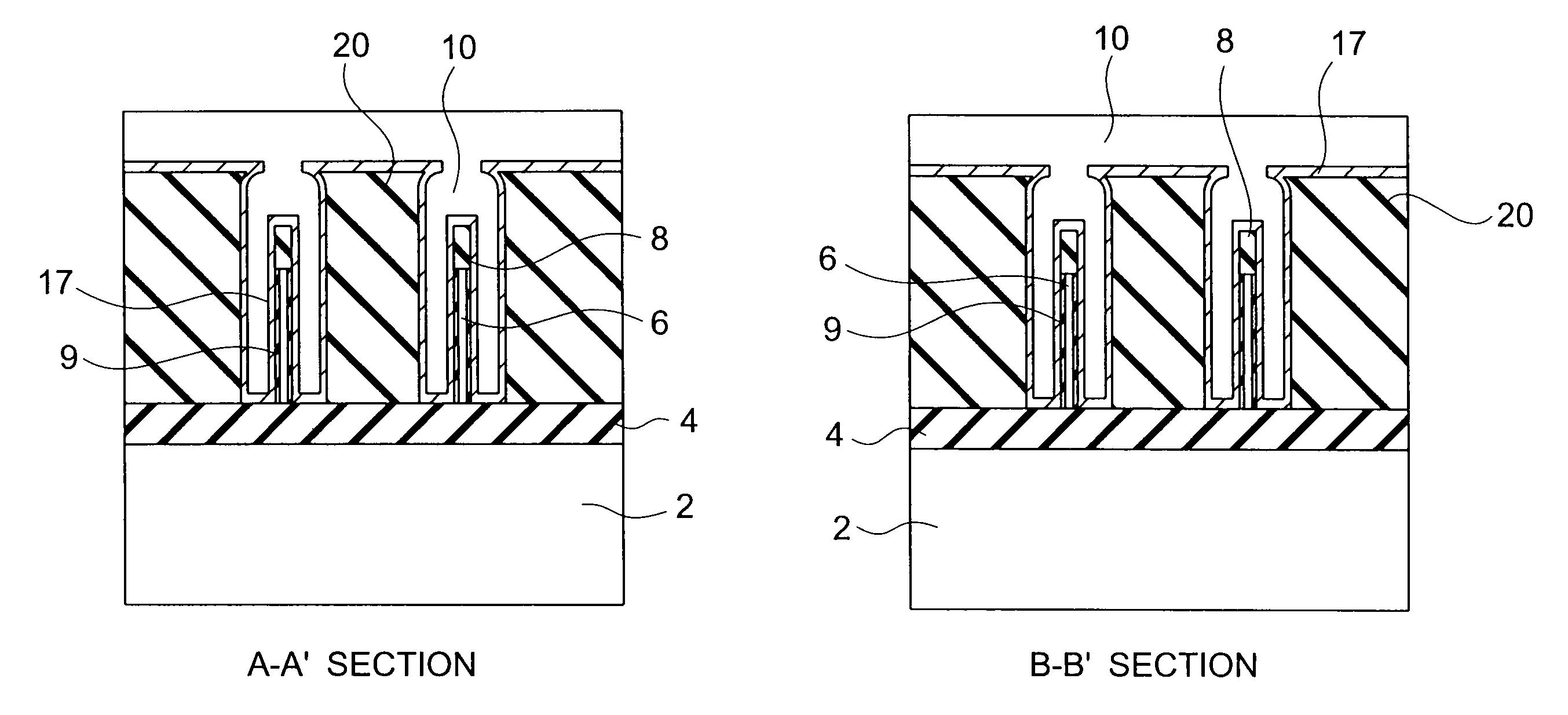
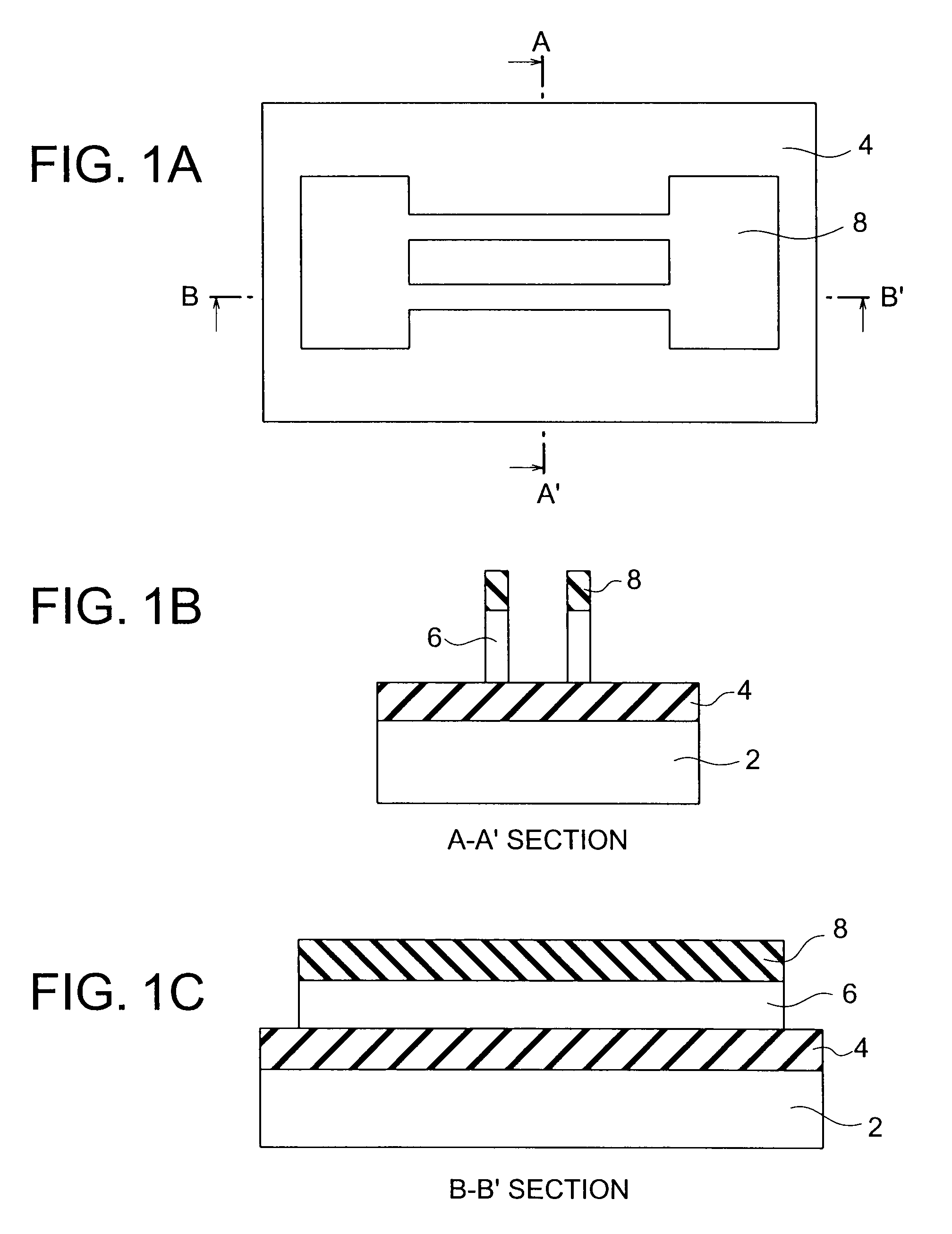
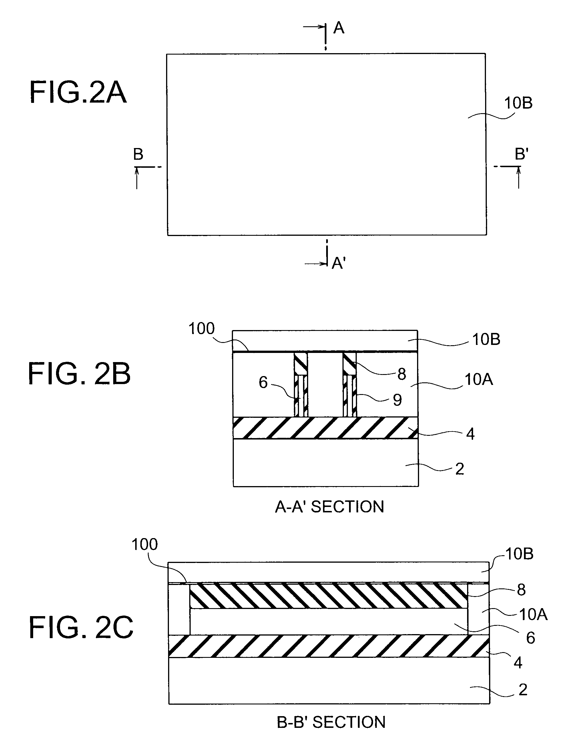
[0046]Referring now to FIGS. 19A to 21D, a method for manufacturing a multi-gate FET in accordance with a second embodiment of the present invention is described. The multi-gate FET manufactured by the method in accordance with this embodiment is of a metal-gate type. FIGS. 19A, 20A, and 21A are cross-sectional views of the multi-gate FET, taken along the line A-A′ of FIG. 6. FIGS. 19B, 20B, and 21B are cross-sectional views of the multi-gate FET, taken along the line B-B′ of FIG. 6. FIGS. 19C, 20C, and 21C are cross-sectional views of the multi-gate FET, taken along the line C-C′ of FIG. 6. FIGS. 19D, 20D, and 21D are cross-sectional views of the multi-gate FET, taken along the line D-D′ of FIG. 6.

[0047]First, the same procedures as the procedures for manufacturing the fully-silicided gate FET of the first embodiment illustrated in FIGS. 7A to 9D are carried out. As shown in FIGS. 19A, 19B, 19C, and 19D, a metal film 17 to be a metal gate is formed by MOCVD (Metal-Organic-Chemical-...


PUM


Abstract

A multi-gate field effect transistor includes: a plurality of semiconductor layers arranged in parallel on a substrate; source and drain regions formed in each of the semiconductor layers; channel regions each provided between the source region and the drain region in each of the semiconductor layers; protection films each provided on an upper face of each of the channel regions; gate insulating films each provided on both side faces of each of the channel regions; a plurality of gate electrodes provided on both side faces of each of the channel regions so as to interpose the gate insulating film, provided above the upper face of each of the channel region so as to interpose the protection film, and containing a metal element; a connecting portion connecting upper faces of the gate electrodes; and a gate wire connected to the connecting portion.

Description

CROSS-REFERENCE TO RELATED APPLICATION[0001]This application is based upon and claims the benefit of priority from prior Japanese Patent Application No. 2008-83680 filed on Mar. 27, 2008 in Japan, the entire contents of which are incorporated herein by reference.BACKGROUND OF THE INVENTION[0002]1. Field of the Invention[0003]The present invention relates to a multi-gate field effect transistor and a method for manufacturing the multi-gate field effect transistor.[0004]2. Related Art[0005]Highly-integrated LSIs with high performances have been achieved by reducing the sizes of field effect transistors (FETs) as the fundamental elements of LSIs and improving the performances of those field effect transistors. The performance of each FET is determined by how high the driving current is during an ON operation and how low the leakage current from the channel is in an OFF state. According to the International Semiconductor Roadmap, novel techniques for realizing higher driving current and...

Claims


Application Information

Patent Timeline
Patent Type & Authority Patents(United States)
IPC IPC(8): H01L21/00
CPCH01L29/66795H01L29/785
Inventor NAKABAYASHI, YUKIOUCHIDA, KEN
Owner KIOXIA CORP
Why Eureka
Try Eureka