Substrate processing apparatus for performing plasma process

a technology of plasma process and processing apparatus, which is applied in the direction of coating, chemical vapor deposition coating, metallic material coating process, etc., can solve the problems of deteriorating process, low process reproducibility, and very expensive parts, so as to achieve uniform temperature distribution during substrate processing, sufficient strength, and low cost

Inactive Publication Date: 2011-10-20
TOKYO ELECTRON LTD
View PDF10 Cites 4 Cited by
  • Summary
  • Abstract
  • Description
  • Claims
  • Application Information

AI Technical Summary

Benefits of technology

An object of the present invention is to provide a substrate processing apparatus including a substrate table and also a substrate table used for the same, which can decrease particles to be generated on the back side of a target substrate placed on the substrate table.
Another object of the present invention is to provide a substrate processing apparatus including a member to be exposed to plasma inside a process container and also a member to be exposed to plasma used for the same, which can practically prevent the member from causing metal contamination.
According to the first and second aspects of the present invention, in a state where the lifter pins is set in the first state on the lower side, the target substrate is held by the lifter pins to be separated from the upper surface of the substrate table. Consequently, the target substrate does not come into direct contact with the substrate table surface, so the particle generation due to this contact is prevented. In this case, the distance of the target substrate from the upper surface of the substrate table in the first state may be set to be within 0.4 mm, so that the uniformity of temperature distribution during a substrate process is kept high.
According to the third to sixth aspects of the present invention, a portion to be exposed to plasma inside the process container is at least partly coated with a silicon film. Typically, a member to be exposed to plasma inside the process container comprises a metal main body and a silicon film that coats the metal main body at least a portion to be exposed to plasma. In this case, the silicon is mainly worn out by plasma, and the aluminum or the like of the metal main body can be hardly worn out, so metal contamination due to e.g., aluminum becomes very few. Further, since formation of the film on the main body of e.g., aluminum is only required, the structure can be provided at a relatively low cost. In addition, the main body is made of a metal, so the sufficient strength is ensured.

Problems solved by technology

However, it has been found that the following problem is caused, where a plasma oxidation process is performed in a microwave plasma processing apparatus including, e.g., the slot antenna described above, while a target substrate is placed on the substrate table 301.
When intense plasma comes into contact with some of these members, the plasma etches the surface of the members and generates particles, which cause metal contamination due to, e.g., aluminum to a large extent, thereby deteriorating the process.
Further, the surface of the members is severely damaged or degraded particularly when the plasma acts on aluminum members, so the process reproducibility becomes lower with a lapse of time in using the apparatus.
However, where the wall portion of a reaction chamber is formed of a processed bulk body of mono-crystalline silicon, this part becomes very expensive but cannot have a sufficient strength, so this is not practical.

Method used


Image

  • Substrate processing apparatus for performing plasma process
  • Substrate processing apparatus for performing plasma process
  • Substrate processing apparatus for performing plasma process

Examples


first embodiment

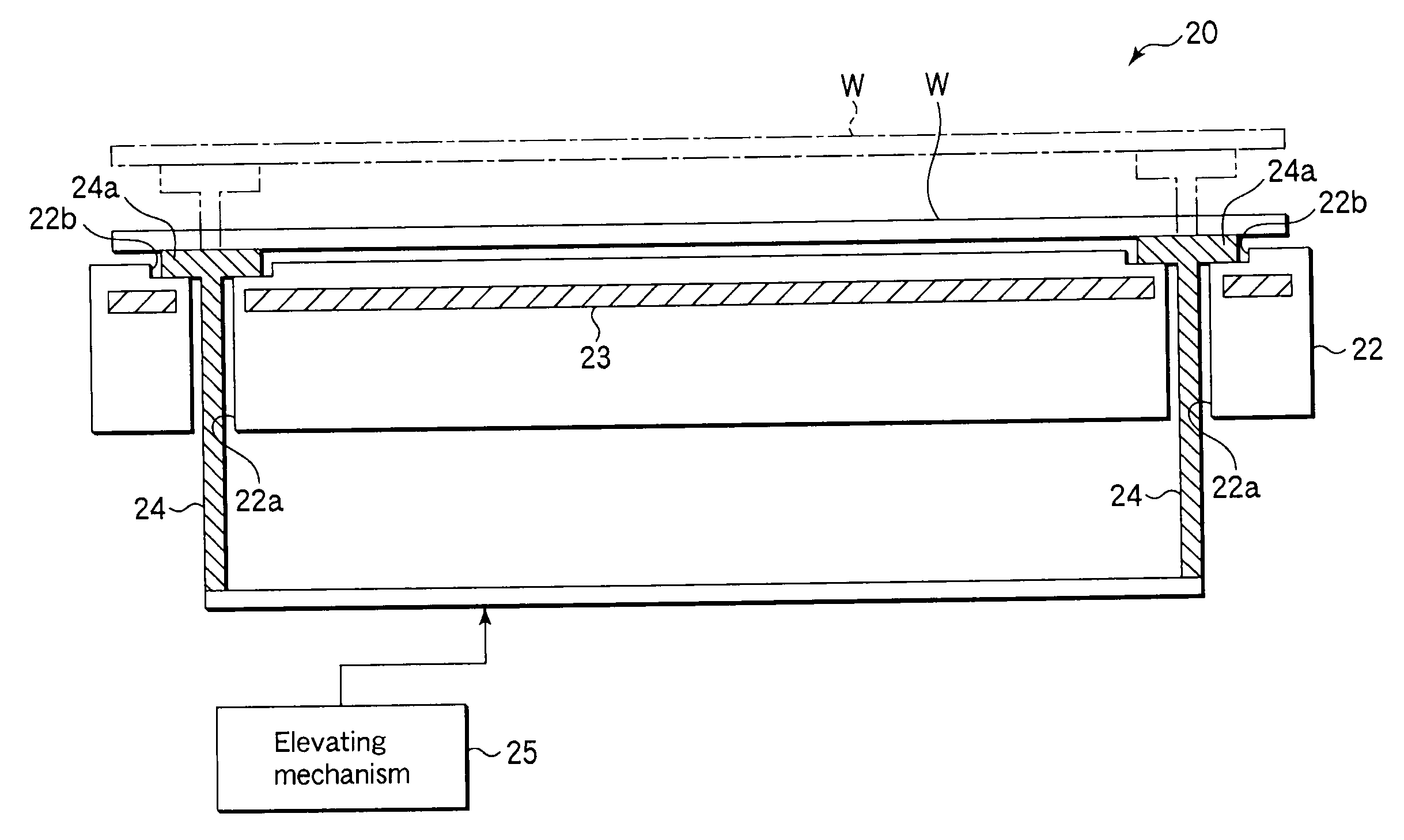
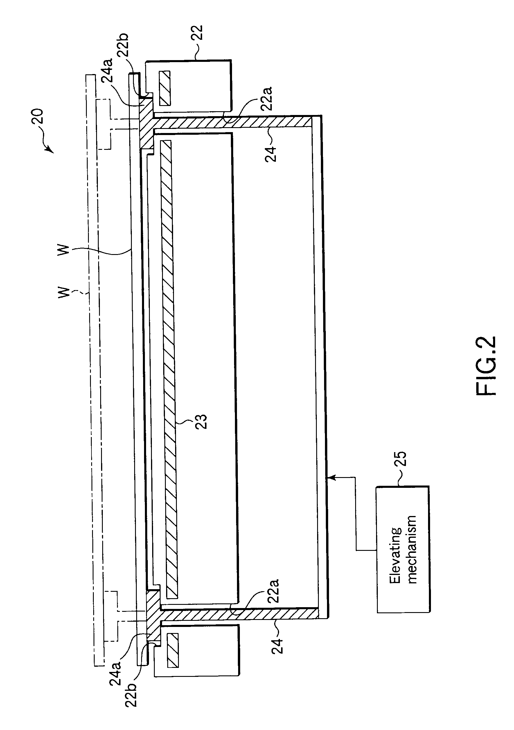
First, a substrate table according to a first embodiment of the present invention will be explained in detail with reference to FIGS. 2 and 3. FIG. 2 is a sectional view showing a substrate table according to this embodiment. FIG. 3 is a plan view of the substrate table shown in FIG. 2. This substrate table may be applied to various substrate processing apparatuses for performing respective processes, such as film formation, etching, and ashing processes. The film formation process is exemplified by a thermal oxidation process, thermal nitridation process, plasma oxidation process, plasma nitridation process, and CVD.

As shown in FIG. 2, a substrate table 20 includes a substrate table main body 22 made of a ceramic material, such as aluminum nitride, in which a heater 23 having a concentric or spiral format is embedded, as shown in FIG. 3. The substrate table main body 22 has through holes 22a formed therein at three positions to insert lifter pins 24 therein. The lifter pins 24 are ...

second embodiment

Next, an explanation will be given of a second embodiment of the present invention.

FIG. 11 is a sectional view schematically showing a plasma processing apparatus according to the second embodiment of the present invention. As in the first embodiment, this plasma processing apparatus 200 is arranged as a plasma processing apparatus, in which microwaves are supplied from a planar antenna having a plurality of slots, such as an RLSA (Radial Line Slot Antenna), into a process chamber to generate plasma, so that microwave plasma is generated with a high density and a low electron temperature.

The plasma processing apparatus 200 includes an airtight chamber (process container) 201 for accommodating a wafer W, wherein the chamber 201 has an essentially cylindrical shape and is grounded. The chamber 201 comprises a housing member 202 made of a metal, such as aluminum or stainless steel, and forming the lower part of the chamber 201, and a chamber wall 203 disposed on the housing member 202....


PUM

PropertyMeasurementUnit
thicknessaaaaaaaaaa
distanceaaaaaaaaaa
diameteraaaaaaaaaa

Abstract

A substrate processing apparatus for performing a plasma process on a target substrate includes a process container configured to accommodate the target substrate. The apparatus includes a gas feed passage configured to supply a process gas into the process container and an exhaust passage configured to exhaust gas from inside the process container. The apparatus further includes a plasma generation mechanism configured to generate plasma of the process gas inside the process container and a metal component to be exposed to plasma inside the process container. The metal component is provided with a silicon film that coats at least a portion thereof to be exposed to plasma and to suffer an intense electric filed generated thereabout.

Description

TECHNICAL FIELD The present invention relates to a substrate processing apparatus for performing a process, such as a plasma process, on a target substrate, such as a semiconductor wafer, and a substrate table and a member to be exposed to plasma used for the same.BACKGROUND ART Conventionally, in the process of manufacturing semiconductor devices, various substrate processes, such as film formation, etching, and ashing processes, are performed on a target object, such as a semiconductor wafer. The film formation process is exemplified by a thermal oxidation process, thermal nitridation process, plasma oxidation process, plasma nitridation process, and CVD.In a substrate process of this kind, a predetermined substrate process is performed at a predetermined substrate temperature on a target substrate, such as a semiconductor wafer, placed on a substrate table disposed in a process container of a substrate processing apparatus. The substrate table is provided with a heater built ther...

Claims


Application Information

Patent Timeline
Patent Type & Authority Applications(United States)
IPC IPC(8): H01L21/3065C23C16/511C23C16/50
CPCC23C16/4586H01L21/68742H01L21/67103H01L21/683
Inventor MURAOKA, SUNAOYAMASHITA, JUNUEDA, ATSUSHI
Owner TOKYO ELECTRON LTD
Why Eureka
Try Eureka