

How to make a capacitor
A manufacturing method and capacitor technology, applied in semiconductor/solid-state device manufacturing, circuits, electrical components, etc., can solve the problems of reducing yield, affecting device quality, metal pollution, etc., to improve quality, avoid metal pollution, and protect electrodes. Effect
- Summary
- Abstract
- Description
- Claims
- Application Information
AI Technical Summary
Problems solved by technology
Method used
Image

Examples
Embodiment Construction
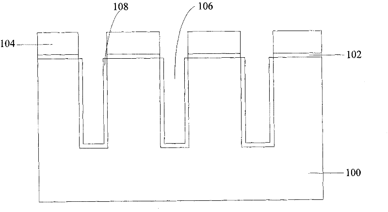
[0016] When using aluminum oxide as a mask to increase the area of the lower part of the deep groove and then increase the usable area of the capacitor, the inventors found that when the first electrode of the capacitor is formed on the side wall and bottom of the enlarged area of the groove, Aluminum oxide will still remain on the upper part of the side wall of the trench as a mask. Since the first electrode is also a conductive material, the metal component in aluminum oxide will cause metal pollution to the first electrode, affecting the quality and conductivity of the first electrode. .
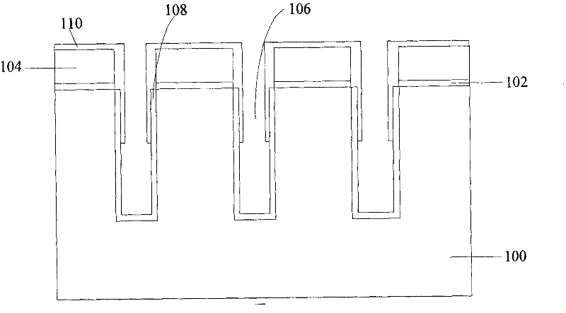
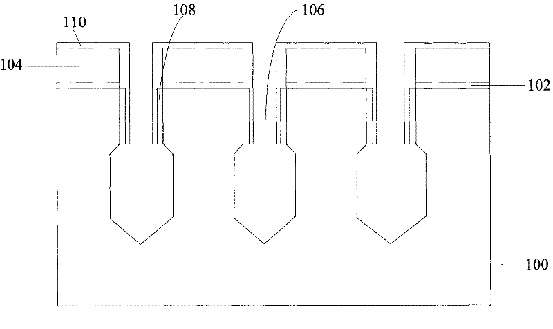
[0017] In view of the above technical problems, the inventor found through experimental research that if a nitride layer is used instead of aluminum oxide as a mask for increasing the trench area, the nitride layer does not contain metal components, thus avoiding the generation of counter electrodes in the subsequent electrode formation process. Metal pollution effectively protects ...
PUM
| Property | Measurement | Unit |
|---|---|---|
| Thickness | aaaaa | aaaaa |
Abstract
Description
Claims
Application Information