Etching method for semiconductor silicon wafer

a silicon wafer and etching technology, applied in the field of semiconductor silicon wafer etching, can solve the problems of mechanical strength, adversely affecting electrical characteristics, and needing to be removed completely

Inactive Publication Date: 2005-01-18
SHIN-ETSU HANDOTAI CO LTD
View PDF12 Cites 3 Cited by
  • Summary
  • Abstract
  • Description
  • Claims
  • Application Information

AI Technical Summary

Benefits of technology

[0009]According to a first aspect of the present invention, an etchant of the present invention is prepared by immersing stainless steel in an alkali aqueous solution for not less than 10 hours. Metallic elements dissolved in such etchant are extremely reduced.
[0014]In the alkali etchant according to the present invention, the concentrations of the iron, nickel, chromium, and copper in the etchant decrease, compared with the alkali etchant without immersing SUS304 or SUS316. As a result, metal contamination of an etching object, for example, a semiconductor wafer, can be reduced, when etching.
[0015]With the alkali etchant according to the present invention, the metal ions existing in the alkali aqueous solution can be unionized by dissolving a reducing agent having a lower oxidation potential compared with the reversible potential of the metal ions existing in the alkali aqueous solution. That is, the metal ions are reduced because the oxidation-reduction potential of the metal ions in the solution may be lower than the oxidation-reduction potential of the reducing agent. Thereby, the amounts of metals residing in the etchant as ions are reduced, so that adhesion of the metal ions to a wafer surface is suppressed. Therefore, the reducing action of the reducing agent is further overlapped with the adsorption deionization effect by the immersion of the stainless steel, so that the effect of further suppression of adhesion of the metal ions to the wafer is exhibited.
[0020]In the alkali etchant, by the reaction product of hydrogen or silicate or the like, which occurs when the silicon material is dissolved, the metal ions in the solution are reduced, or bonded to the silicate or the like, so that the amounts of residing as ions are reduced. This will further heighten the effect of immersing stainless steel or the effect of adding a reducing agent.
[0021]The etchant of the present invention is prepared in a container. At least the portion of the container that is in contact with the alkali solution is made from an alkali resistant material, for example, polypropylene. Thereby, since there is little elution of metallic elements from the material of the container, consequently, it is effective for suppressing adhesion of the metal ions to a wafer without rising of the concentrations of the metal ions in the alkali aqueous solution.
[0023]According to a second aspect of the present invention, an etching method of the present invention is the one that etching of a semiconductor silicon wafer is carried out by using the above-described etchant. According to the etching method, metal contamination of the semiconductor silicon wafer is prevented effectively.

Problems solved by technology

In a manufacturing process of devices, since the process damage layer induces a crystal defect, such as slip dislocation, lowers mechanical strength of a wafer, and also affects adversely on electrical characteristic, it is required to be removed completely.
Therefore, as a material of an etching vessel, for example, even if it is the case that polypropylene is used in consideration of corrosion resistance, the silicon wafer is contaminated by the iron, nickel, chromium, and copper or the like, which are included in the alkali aqueous solution.
However, even by these methods, the amount of contamination of the metallic elements adhering to or being diffused inside an etched wafer, is still a problem for manufacturing the latest high integration device.

Method used


Image

  • Etching method for semiconductor silicon wafer
  • Etching method for semiconductor silicon wafer
  • Etching method for semiconductor silicon wafer

Examples


example

[0027]1. Method for Preparing Etchant

[0028](1) Treatment of Immersing Stainless Steel in Etchant

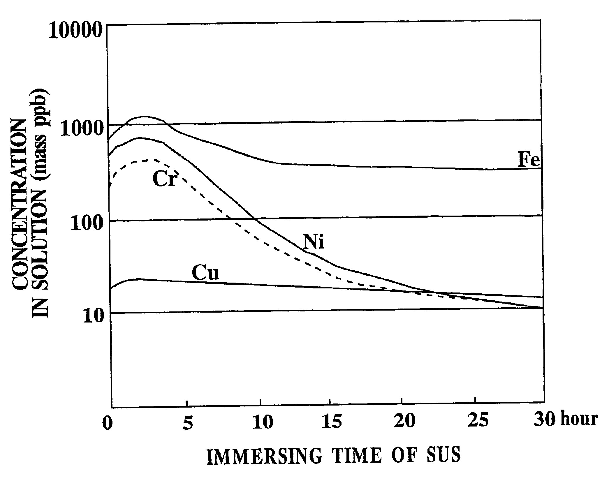
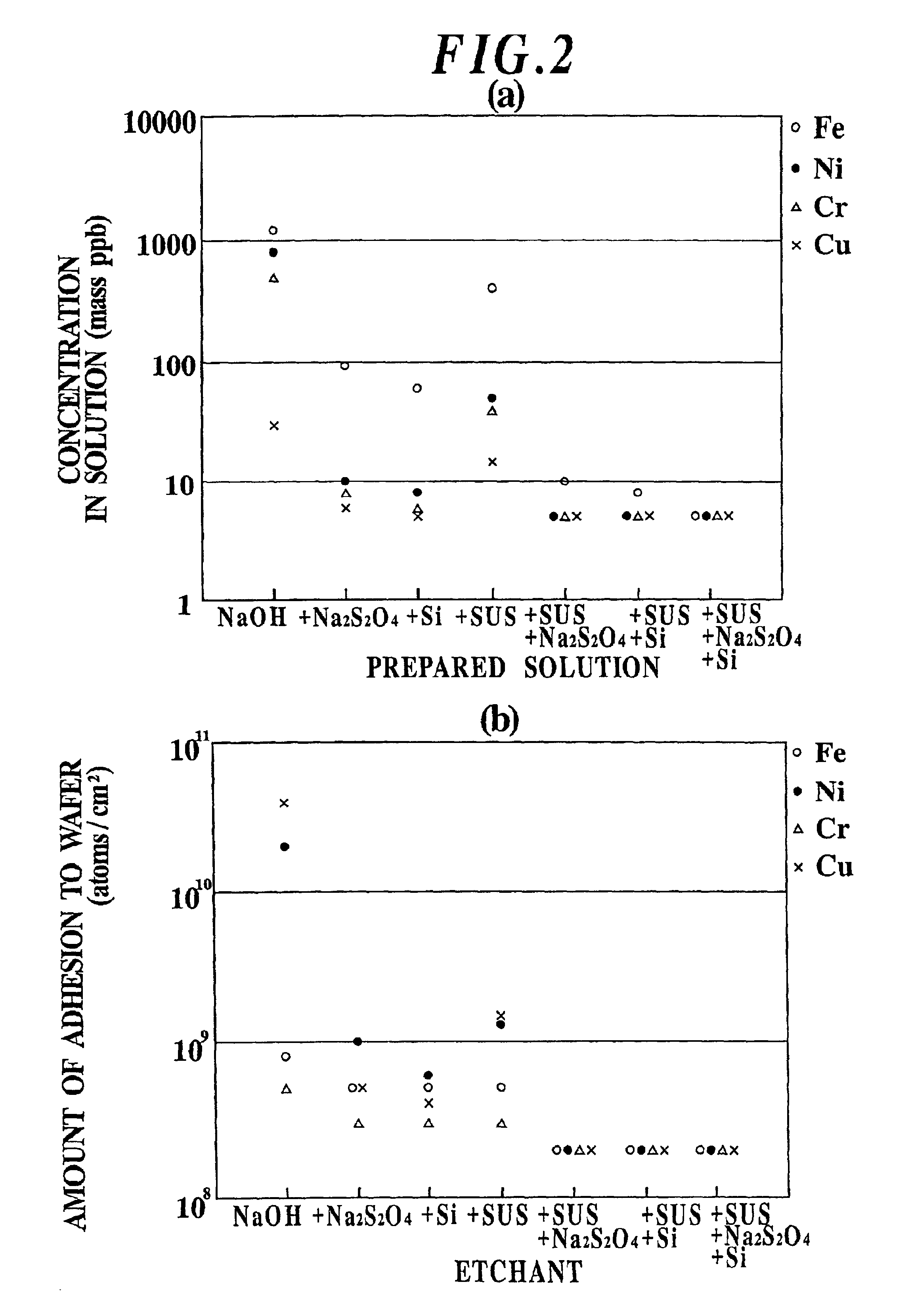
[0029]Into a tank made from polypropylene, 20 liters of sodium hydroxide (45% by mass for industry) was put in. After raising temperature to a predetermined temperature (85° C.), while keeping at 85±1° C., a plate (30 cm in length, 10 cm in width, and 0.2 mm in thickness) of SUS316 having a fresh metal surface was immersed so that both surfaces thereof would be in contact with the sodium hydroxide aqueous solution. Then, after a predetermined time is passed, the SUS316 was taken out.

[0030](2) Adding Dithionite

[0031]A predetermined amount (100 g) of sodium dithionite was added to the sodium hydroxide aqueous solution, which was prepared in said (1) by treatment of immersing SUS, and dissolved therein.

[0032](3) Dissolving Silicon

[0033]A predetermined amount (100 g) of Si was added to the sodium hydroxide aqueous solution, which was prepared in said (1) by treatment of immersing SUS, and dis...


PUM

PropertyMeasurementUnit
temperatureaaaaaaaaaa

Abstract

An etchant and an etching method that contribute to prevention of metal contamination of a semiconductor silicon wafer, and a semiconductor silicon wafer in which metal contamination is extremely reduced, are provided. The etchant according to the present invention is prepared by immersing stainless steel in an alkali aqueous solution for not less than 10 hours. In the etching method according to the present invention, a semiconductor silicon wafer is etched by using the etchant. Thereby, the semiconductor silicon wafer according to the present invention, in which metal contamination is extremely reduced, is obtained.

Description

TECHNICAL FIELD[0002]The present invention relates to a semiconductor material, particularly, to an etchant, an etching method of a silicon wafer, and a semiconductor silicon wafer.BACKGROUND ART[0003]A silicon wafer passed through machining processes of block cutting, outer diameter grinding, slicing, and lapping, has a damaged layer, that is, an process damage layer, on the surface. In a manufacturing process of devices, since the process damage layer induces a crystal defect, such as slip dislocation, lowers mechanical strength of a wafer, and also affects adversely on electrical characteristic, it is required to be removed completely.[0004]Conventionally, removing the process damage layer, which is introduced into a silicon wafer in the machining processes, by chemical etching, is carried out. As methods of the chemical etching, there are acid etching and alkali etching. Among these, the alkali etching has few problems in occurrence of a harmful by-product, such as NOx in the ac...

Claims


Application Information

Patent Timeline
Patent Type & Authority Patents(United States)
IPC IPC(8): C11D11/00C11D7/06C11D7/02H01L21/02H01L21/306C01D1/28C30B29/06C30B33/08
CPCC01D1/28C11D7/06H01L21/30608H01L21/02019H01L21/30604C11D11/0047H01L21/3063
Inventor MIYAZAKI, SEIICHI
Owner SHIN-ETSU HANDOTAI CO LTD
Why Eureka
Try Eureka